Note
Go to the end to download the full example code
Fixing sharp angles in the layout of a directional coupler
This example shows how to use layout operations to stub acute angles that are found in the layout of a directional coupler. Stubbing acute angles is an important step in the design process in order to make sure that your device passes the design rule checks (DRCs) of a foundry or fab.
First we import a directional coupler from picazzo:
import si_fab.all as pdk # noqa
import ipkiss3.all as i3
from picazzo3.traces.wire_wg import WireWaveguideTemplate
from picazzo3.wg.dircoup.cell import BendDirectionalCoupler
dc = BendDirectionalCoupler(
name="myDC",
trace_template1=WireWaveguideTemplate(),
trace_template2=WireWaveguideTemplate(),
)
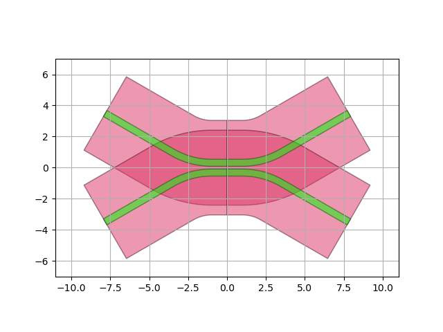
dc_lay = dc.Layout(
manhattan=False,
straight_after_bend=5.0,
bend_angle=30,
)
dc_lay.visualize()
<Figure size 640x480 with 1 Axes>
The layout can be checked on acute angles using get_acute_angle_points:
acute_points = i3.get_acute_angle_points(dc_lay)
for layer in acute_points:
    for point_data in acute_points[layer]:
        point, _, angle = point_data
        print(
            "Acute point ({:.2f}, {:.2f}) with a {:.2f} degree angle found in layer {}".format(
                point[0], point[1], angle, layer
            )
        )
Acute point (7.72, -3.68) with a 89.98 degree angle found in layer PPLAYER SI-DRW
Acute point (-7.72, -3.68) with a 89.98 degree angle found in layer PPLAYER SI-DRW
Acute point (7.72, 3.68) with a 89.98 degree angle found in layer PPLAYER SI-DRW
Acute point (-7.72, 3.68) with a 89.98 degree angle found in layer PPLAYER SI-DRW
Acute point (7.25, 0.00) with a 299.99 degree angle found in layer PPLAYER SI-UNUSED
Acute point (-9.19, 1.13) with a 89.99 degree angle found in layer PPLAYER SI-UNUSED
Acute point (-7.24, 0.00) with a 300.01 degree angle found in layer PPLAYER SI-UNUSED
Acute point (-9.19, -1.13) with a 89.99 degree angle found in layer PPLAYER SI-UNUSED
Rounding errors and grid snapping have caused some 90-degree angles to be slightly acute. Since these are not angles that need to be stubbed, the angle_threshold argument can be used to avoid this.
acute_points = i3.get_acute_angle_points(dc_lay, angle_threshold=0.1)
for layer in acute_points:
    for point_data in acute_points[layer]:
        point, _, angle = point_data
        print(
            "Acute point ({:.2f}, {:.2f}) with a {:.2f} degree angle found in layer {}".format(
                point[0], point[1], angle, layer
            )
        )
Acute point (7.25, 0.00) with a 299.99 degree angle found in layer PPLAYER SI-UNUSED
Acute point (-7.24, 0.00) with a 300.01 degree angle found in layer PPLAYER SI-UNUSED
The stub elements can be inspected using get_stub_elements:
elems_add, elems_subt = i3.get_stub_elements(dc_lay, angle_threshold=0.1, stub_width=0.5)

stubs_lay = i3.LayoutCell().Layout(elements=elems_add + elems_subt)
stubs_lay.visualize()
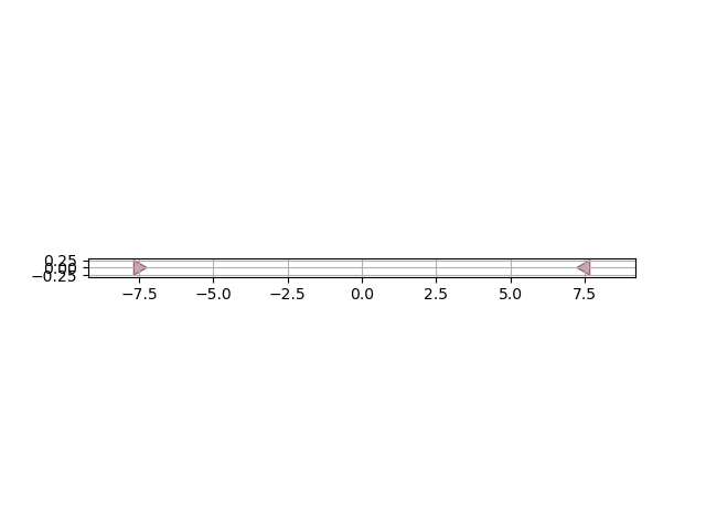
<Figure size 640x480 with 1 Axes>
In some cases the stub elements turn out to be too small due to grid snapping. Therefore, it is also possible to specify the grow_amount argument:
elems_add, elems_subt = i3.get_stub_elements(
    dc_lay,
    angle_threshold=0.1,
    stub_width=0.5,
    grow_amount=0.5,
)

stubs_lay = i3.LayoutCell().Layout(elements=elems_add + elems_subt)
stubs_lay.visualize()
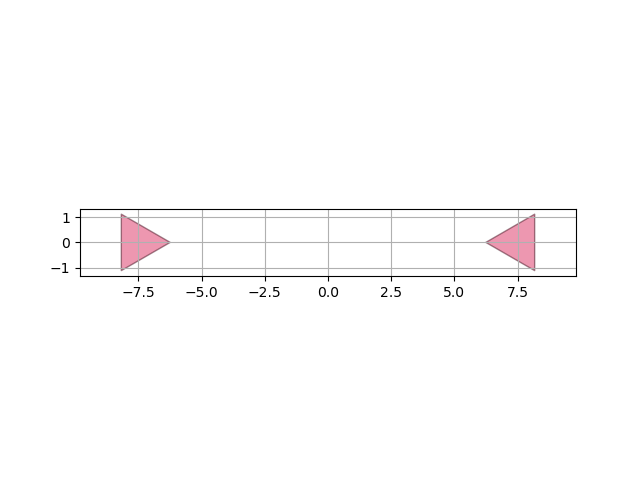
<Figure size 640x480 with 1 Axes>
To stub the acute angles and create the new layout we can use stub_acute_angles. There are several ways to do this:
By default, all acute angles on all layers are stubbed.
elems = i3.stub_acute_angles(
    dc_lay,
    angle_threshold=0.1,
    stub_width=0.5,
)
stubbed_layout = i3.LayoutCell().Layout(elements=elems, ports=dc_lay.ports)
Specify which stub elements to add and subtract using the stub_elements argument.
elems = i3.stub_acute_angles(dc_lay, stub_elements=[elems_add, elems_subt])
stubbed_layout = i3.LayoutCell().Layout(elements=elems, ports=dc_lay.ports)
Specify the layer(s) on which to stub the acute angles.
elems = i3.stub_acute_angles(
    dc_lay,
    angle_threshold=0.1,
    stub_width=0.5,
    layers=[i3.PPLayer(i3.TECH.PROCESS.SI, i3.TECH.PURPOSE.LF_AREA)],
)
stubbed_layout = i3.LayoutCell().Layout(elements=elems, ports=dc_lay.ports)
In certain situations a combination of the previous two methods might be useful. The three examples above give the same result.
stubbed_layout.visualize()
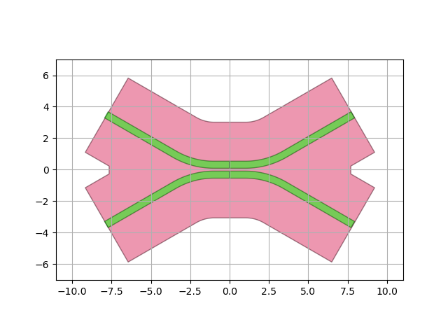
<Figure size 640x480 with 1 Axes>
It is important to note that stub_acute_angles does a flatten + merge operation on the full layout.
Hence, it is not recommended to perform this function on a large design due to performance reasons and also because
by flattening a large design you lose all hierarchy.
This leads to an increased GDS file size which makes it harder to navigate the final design.
In addition, some foundries use black box cells that should not be flattened.
The recommended way to fix DRC errors is to fix them as ‘locally’ as possible (i.e., in the pcell where they occur).
If that is not possible, you can still use i3.get_stub_elements
on the full circuit (be mindful of the performance impact) and add the elements to the final design using LayoutCell
(check out the documentation of i3.get_stub_elements for more information).