Schematic capture in IPKISS Canvas
IPKISS Canvas is your design copilot that works alongside the other Luceda tools to enable a comprehensive photonic design flow. In the previous tutorial we have already seen how it can be used to verify existing layouts. Here, we will explore how it can be used as a schematic capture tool and assist with creating new circuits.
But first, what is a schematic?
At a basic level, it is a visual representation of a circuit in which components and sub-circuits are simplified into single blocks, and the top-level circuit represents the connections between these blocks. It is not a physical layout with structures, waveguides and dimensions, but rather an abstracted view that focuses on logical connections and uses icons to represent components and sub-circuits. Removing these constraints enables us to more clearly see the circuit design without having to worry about the exact layout implementation.
Schematic capture is then simply the process of converting a design idea into such a schematic. In Canvas this takes the shape of a workspace that is populated by blocks and connections. These blocks represent instances, which can be a components or sub-circuits, each having its own hierarchy. Each instance has properties, parameters and metadata that enable you to explore the design in an intuitive way.
Schematic generation
The first step is to create our project. This is done by opening the Luceda Control Center (LCC) that came with your Luceda installation and clicking on the ‘IPKISS Canvas’ button.
Next, select ‘New Project’ and follow the instructions. We are also going to import the si_fab PDK, which can be found at C:/Users/[NAME]/luceda/luceda_academy/luceda[VERSION]/pdks/si_fab/ipkiss/si_fab/si_fab.iclib. In Canvas, you can import every supported PDK using its corresponding ‘.iclib’ file.
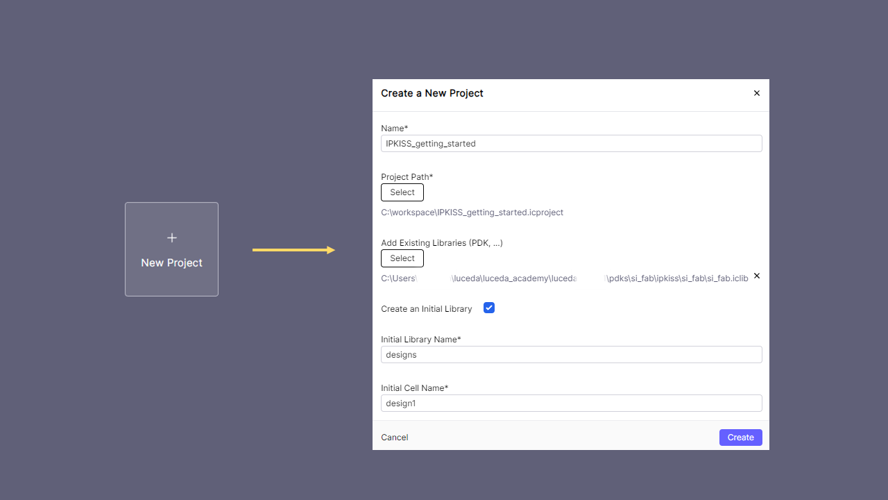
Creating a new IPKISS Canvas design project
From here we can drag and drop the components we need into the workspace, and connect the terms (which represent the physical optical or electrical ports) by clicking on the term pairs to form connections. These connections are not waveguides, but can be thought of as logical connections between terms in our circuit.
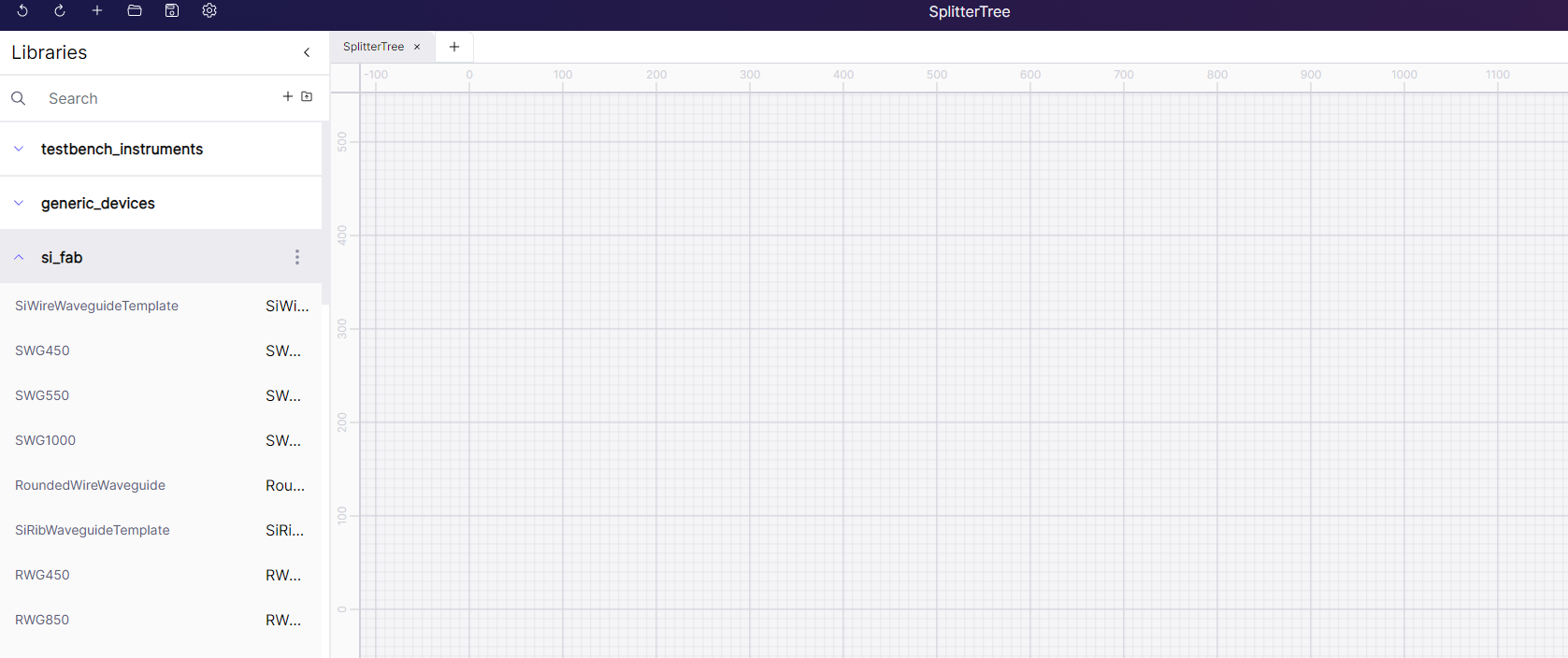
Exploring PDK components
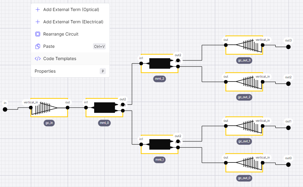
Try to recreate the circuit we saw in the circuit layout part of this Getting Started using the MMI1x2Optimized1550 and FC_TE_1550 components.
By right-clicking in Canvas and selecting Rearrange Circuit, it will automatically try to arrange the components and connections in a sensible structure.
If you want to further modify the layout you can drag and drop cells to move them around, or if you select multiple cells at once, you can make use of the alignment options in the right-click menu.
So far we have only used fixed cell components, which have no parameters exposed to the user.
If you replace one of the MMI1x2Optimized1550 components with an MMI1x2, then right-click and press Properties, the Properties tab wil be populated with the different options.
These correspond to all the top-level and layout parameters you can pass into the class in code, and is a great way to explore all the options available to you.
Once you have added all the components and connections you want, your circuit is complete.
Creating a circuit and selecting a code template
Code templates
Canvas already helps you write IPKISS code by visualizing library components with their port names and properties. On top of that, Canvas can jump-start your designs by generating code from a schematic using ‘code templates’. A code template refers to how we map between a schematic circuit and the code we generate to describe it.
Once you have finished creating a circuit, you can right-click on the workspace and use the </> Code Template option to browse the available code templates.
Some are supplied by default with IPKISS, but you can create your own as well.
Using the ‘i3.Circuit (i3.ConnectManhattan/i3.ConnectElectrical)’ code template, we will generate code for this circuit and copy it into our code editor. Open the python file that’s part of this chapter, 1_generated_code.py, to view the result.
Code completion
The code generated by Canvas provides a useful starting point. However, it may require some optimization improvements to complete your design. First of all, the code is not parametric, so it is only useful for creating the exact same circuit. By adding some properties to the class, and using Python logic where possible, we can create a reusable class in line with the circuits we saw in the circuit layout section.
We start by seeing there are no properties in the exported code, so we would want to add properties to describe our circuit.
class GeneratedSplitterTree(i3.Circuit):
    def _default_insts(self):
        # Variable names are auto-generated.
        # You can use the refactoring feature of your IDE to change them to more meaningful names.
        # Parameters will always be passed to the top level PCell, not to its view.
        # Therefore, you should make the necessary changes and pass the parameters accordingly.
        mmi1x2optimized1550_1 = si_fab.MMI1x2Optimized1550()
        fc_te_1550_2 = si_fab.FC_TE_1550()

        return {
            "mmi_0": mmi1x2optimized1550_1,
            "mmi_2": mmi1x2optimized1550_1,
            "mmi_1": mmi1x2optimized1550_1,
            "gc_in": fc_te_1550_2,
            "gc_out_0": fc_te_1550_2,
            "gc_out_1": fc_te_1550_2,
            "gc_out_2": fc_te_1550_2,
            "gc_out_3": fc_te_1550_2,
        }
In this case the circuit is the same as in the previous section, so we would add some component spacing (as PositiveNumberProperty), as well as child cell properties for the splitters and grating couplers.
We could also use a for-loop to add multiple instances at once.
Next we see that all the connected ports in the schematic have been connected using ConnectManhattan.
If there are no further parameters we want to pass to the connector (such as bend radius or bending algorithm) then this step can be reduced to passing in a single list of the connected ports, all at the same time.
            i3.ConnectManhattan("gc_in:out", "mmi_0:in1"),
            i3.ConnectManhattan("mmi_0:out2", "mmi_2:in1"),
            i3.ConnectManhattan("mmi_0:out1", "mmi_1:in1"),
            i3.ConnectManhattan("mmi_2:out2", "gc_out_3:out"),
            i3.ConnectManhattan("mmi_2:out1", "gc_out_2:out"),
            i3.ConnectManhattan("mmi_1:out2", "gc_out_1:out"),
            i3.ConnectManhattan("mmi_1:out1", "gc_out_0:out"),
The code template that we used to generate this code creates placements for all the instances from their coordinates in Canvas.
This is unlikely to result in a photonic circuit that works, and makes it very slow to change the layout if we need to move instances around (for example to accommodate larger bend radii).
Again we should aim to replace all of these arbitrary numbers with properties that have a well defined meaning (like the spacing between components), and use PlaceRelative where one instance is dependent on the position of another.
            i3.Place("mmi_0", (140, 580), angle=0),
            i3.Place("mmi_2", (300, 700), angle=0),
            i3.Place("mmi_1", (300, 460), angle=0),
            i3.Place("gc_in", (0, 580), angle=0),
            i3.Place("gc_out_0", (540, 410), angle=180),
            i3.Place("gc_out_1", (540, 520), angle=180),
            i3.Place("gc_out_2", (540, 630), angle=180),
            i3.Place("gc_out_3", (540, 750), angle=180),
        ]
Finally we check the exposed ports. This code will work, however we might want to have a more sensible order of the exposed ports. We can accomplished this using a small loop depending on how many ports there are.
    def _default_exposed_ports(self):
        return {
            "gc_out_3:vertical_in": "out3",
            "gc_out_2:vertical_in": "out2",
            "gc_out_1:vertical_in": "out1",
            "gc_out_0:vertical_in": "out0",
            "gc_in:vertical_in": "in",
        }
Now we have seen how a circuit can be quickly prototyped in Canvas, before moving back into code to finalize the details. Of course using Canvas does not stop there. It is a great tool for navigating and verifying the circuit cell you have just been working on.
More information
For an in-depth guide to Canvas, visit IPKISS Canvas.
For a tutorial on how to use Canvas to explore and verify your design, visit Routed OPA: verification, visualization, and simulation.