Note
Go to the end to download the full example code
Running a CAMFR simulation to compute the field profiles
This sample illustrates how to setup a CAMFR simulation and compute the field distributions in your device.
The example starts from a layout defined for a custom TECHNOLOGY.
Note
A custom technology is not a requirement for the CAMFR simulator to work.
Illustrates
how to compute the wavelength and polarisation/mode dependent effective index
how to discretize a structure and define the CAMFR input
how to extract the simulated fields
Getting started
We start by importing camfr with other required modules:
import ipkiss3.all as i3
import numpy as np
import matplotlib.pyplot as plt
import camfr
The fabrication processes are specified in a TechnologyTree with a VFabricationProcessFlow.
For more details on defining a custom technology see also the
Technology guide.
from ipkiss.visualisation.display_style import DisplayStyle
from ipkiss.technology.technology import TechnologyTree
The Environment object is needed to specify the wavelength of interest.
from ipkiss.visualisation.color import Color

COLOR_LIGHT_BLUE = Color(name="Lightblue", red=0.78, green=0.84, blue=0.91)
COLOR_LIGHT_RED = Color(name="Lightred", red=0.9, green=0.4, blue=0.4)
COLOR_DARK_BLUE = Color(name="Darkblue", red=0.58, green=0.7, blue=0.91)
Defining the technology Materials and Virtual Fabrication
layer_wg = i3.Layer(0)
layer_rib = i3.Layer(1)
layer_clad = i3.Layer(2)

process_wg = i3.ProcessLayer(name="wg", extension="wg")
process_rib = i3.ProcessLayer(name="rib", extension="rib")

si = i3.Material(name="silicon", display_style=DisplayStyle(color=COLOR_LIGHT_RED), epsilon=3.45**2)
ox = i3.Material(name="oxide", display_style=DisplayStyle(color=COLOR_LIGHT_BLUE), epsilon=1.45**2)
mat_fact = i3.MaterialFactory()
mat_fact.si = si
mat_fact.ox = ox

i3.TECH.MATERIALS = mat_fact

soi = i3.MaterialStack(
    name="soi", materials_heights=[(ox, 2.0), (si, 0.22), (ox, 2.0)], display_style=DisplayStyle(color=COLOR_LIGHT_RED)
)
soi_etched = i3.MaterialStack(
    name="soi_etched",
    materials_heights=[(ox, 2.0), (si, 0.15), (ox, 0.07), (ox, 2.0)],
    display_style=DisplayStyle(color=COLOR_DARK_BLUE),
)
allox = i3.MaterialStack(
    name="all oxide",
    materials_heights=[(ox, 2.0), (ox, 0.22), (ox, 2.0)],
    display_style=DisplayStyle(color=COLOR_LIGHT_BLUE),
)

matstack_fact = i3.MaterialStackFactory()
matstack_fact.soi = soi
matstack_fact.soi_etched = soi_etched
matstack_fact.allox = allox
Mapping the material stacks
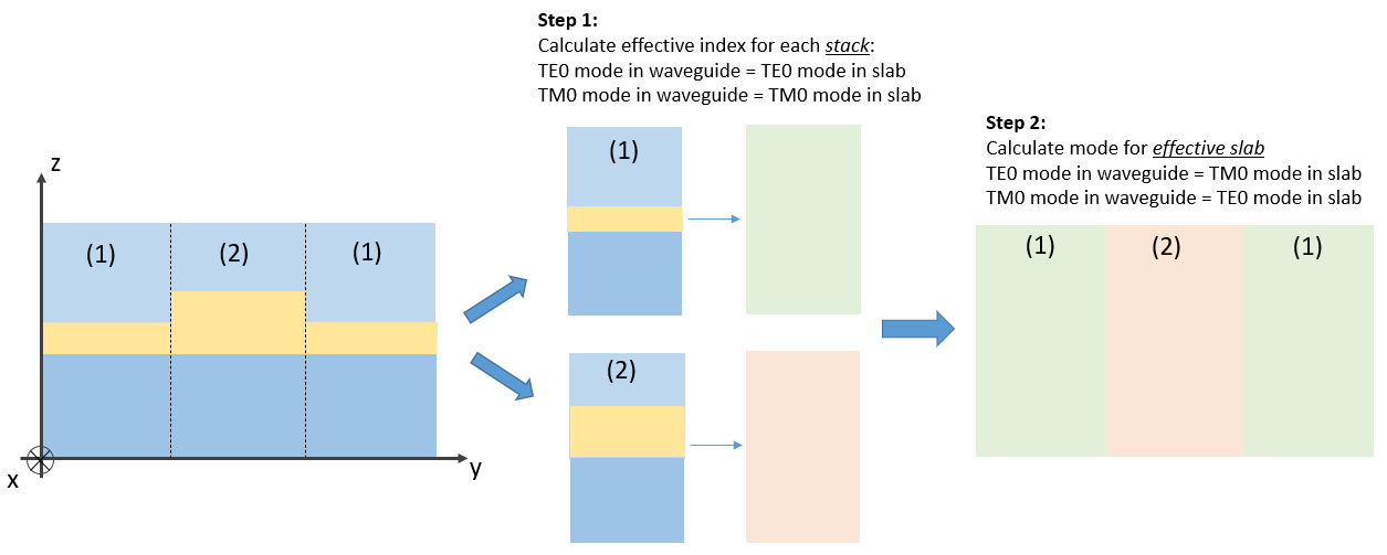
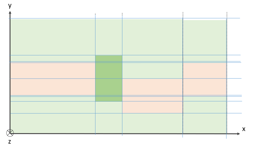
Converting a 2D cross-section of a waveguide into a 1D effective slab
For an arbitrary waveguide cross section we rely on the effective index approach to convert an essentially 2D problem into a 1D by defining an effective slab that is infinite along one direction. Each of the stack (labelled with 1 and 2 in Fig. Converting a 2D cross-section of a waveguide into a 1D effective slab) is converted to an effective material with the new (effective) index of refraction. Additionally, the modes are switched, so TE modes in the original structure become TM modes in CAMFR and the other way round.
To compute the effective indices we invoke
i3.device_sim.camfr_compute_stack_neff,
which requires an environment to account for the wavelength dispersion of our device and materials,
and the name of the mode.
This computation has to be performed for each MaterialStack.
Instead of providing purely a value for the effective index, we’re providing an effective Material, which leaves
an option of creating a model that can depend on environment parameters (for example, a wavelength dependence).
material_stack_to_material_map = dict()
wavelength = 1.55
environment = i3.Environment(wavelength=wavelength)
for _, ms in matstack_fact:
    neff = i3.device_sim.camfr_compute_stack_neff(ms, environment=environment, mode="TE0")
    material_stack_to_material_map[ms] = i3.Material(name="effective_" + ms.name, epsilon=neff.real**2)
Furthermore, if we are not satisfied with the computed effective index, we can either limit the domain of the
computation by limiting (‘clipping’) our stack, or even overwrite the value.
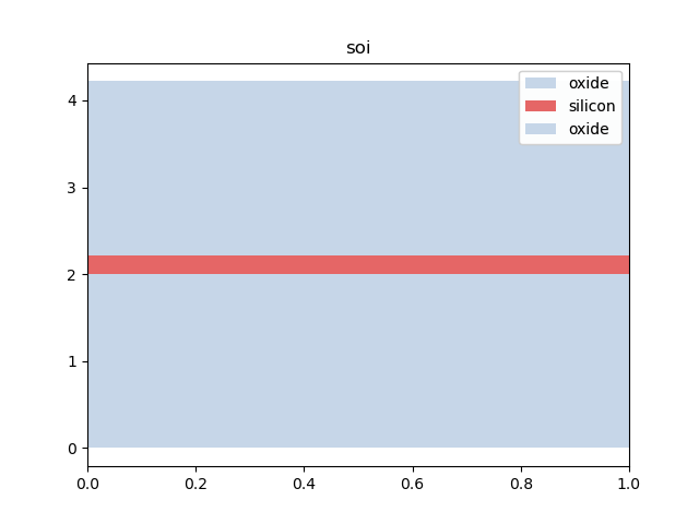
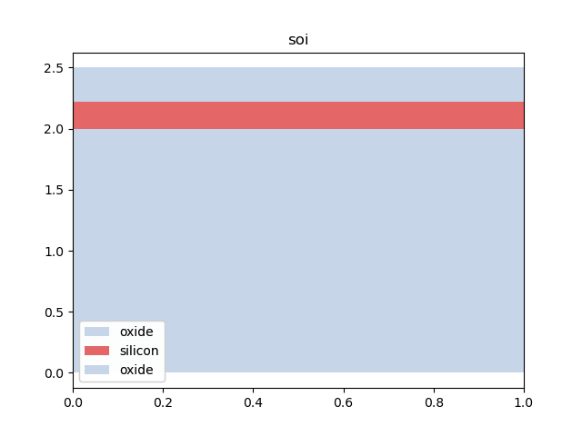
Visual representation of a stack mstack.visualize() might help to choose the limits.
soi.visualize()

clipped_soi = soi.clip_copy(z_min=0, z_max=2.5)
clipped_soi.visualize()
neff = i3.device_sim.camfr_compute_stack_neff(clipped_soi, environment=environment, mode="TE0")
material_stack_to_material_map[soi] = i3.Material(name="effective_" + soi.name, epsilon=neff.real**2)
material_stack_to_material_map[allox] = i3.Material(name="effective_" + allox.name, epsilon=1.45**2)
Defining the layout
Next we define the layout of an MMI
vfab = i3.VFabricationProcessFlow(
    active_processes=[process_wg, process_rib],
    process_layer_map={process_wg: layer_wg, process_rib: layer_rib},
    process_to_material_stack_map=[
        ((0, 0), allox),
        ((1, 0), soi),
        ((0, 1), soi_etched),
        ((1, 1), soi),
    ],
    is_lf_fabrication={process_wg: False, process_rib: False},
)

i3.TECH.VFABRICATION = TechnologyTree()
i3.TECH.VFABRICATION.PROCESS_FLOW = vfab

mmi = i3.LayoutCell(name="mmi").Layout(
    elements=[
        i3.Line(layer=layer_wg, begin_coord=(0.0, 0.0), end_coord=(10.0, 0.0), line_width=0.5),
        i3.Line(layer=layer_wg, begin_coord=(10.0, 0.0), end_coord=(19.9, 0.0), line_width=2.9),
        i3.Line(layer=layer_wg, begin_coord=(19.9, 0.5 + 0.25), end_coord=(29.9, 0.5 + 0.25), line_width=0.5),
        i3.Line(layer=layer_wg, begin_coord=(19.9, -0.5 - 0.25), end_coord=(29.9, -0.5 - 0.25), line_width=0.5),
        i3.Wedge(layer=layer_rib, begin_coord=(0.0, 0.0), end_coord=(5.0, 0.0), begin_width=0.5, end_width=1.2),
        i3.Line(layer=layer_rib, begin_coord=(5.0, 0.0), end_coord=(24.9, 0.0), line_width=6.0),
        i3.Wedge(
            layer=layer_rib,
            begin_coord=(24.9, 0.5 + 0.25),
            end_coord=(29.9, 0.5 + 0.25),
            begin_width=1.2,
            end_width=0.5,
        ),
        i3.Wedge(
            layer=layer_rib,
            begin_coord=(24.9, -0.5 - 0.25),
            end_coord=(29.9, -0.5 - 0.25),
            begin_width=1.2,
            end_width=0.5,
        ),
        i3.Line(layer=layer_clad, begin_coord=(0.0, 0.0), end_coord=(29.9, 0.0), line_width=6.0),
    ]
)
which can be visualized,
mmi.visualize()
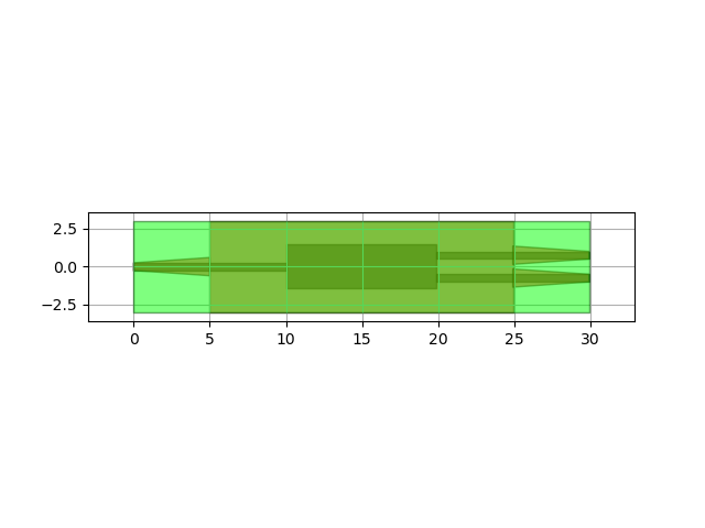
<Figure size 640x480 with 1 Axes>
together with the virtually fabricated structure.
mmi.visualize_2d(process_flow=vfab)
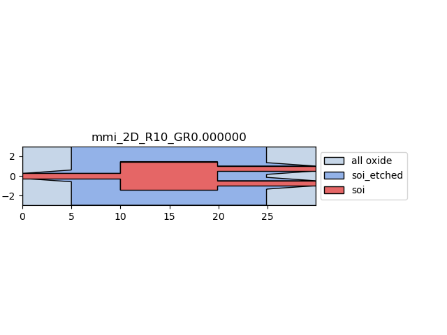
<Figure size 640x480 with 1 Axes>
Defining the CAMFR simulation
Setting the CAMFR parameters requires specifying the wavelength,
camfr.set_lambda(wavelength)
the number of modes,
camfr.set_N(20)
and the polarisation of the light. Notice that we specify camfr.TM polarisation because TM in the effective slab
is equivalent to TE in the original structure.
camfr.set_polarisation(camfr.TM)
Before invoking the actual simulation we have to discretize our structure to provide an input
for the camfr.Stack(), which is a CAMFR object that defines the simulation.
We have already converted a 2D cross section to 1D by using the effective index method.
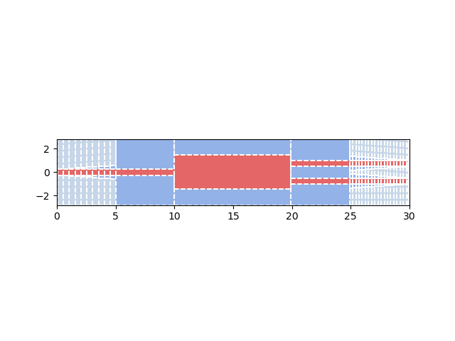
The discretization is performed to convert a longitudinally varying structure into a set of finite size (effective)
slabs,
Discretization of a longitudinally varying structure
as shown in Fig. Discretization of a longitudinally varying structure.
To do so we use the function
i3.device_sim.camfr_stack_expr_for_structure,
which requires the following parameters:
1 / discretisation_resolutiondefines what is the minimal change between the widths and lengths of consecutive needed for a new slab to be created.window_size_infois optional serves to limit the computational domain.process_flowandmaterial_stack_factoryare also optional and serve to define a custom virtual fabrication.
More importantly, we need to provide the material_stack_to_material_map for every MaterialStack
from the TECHNOLOGY that we use.
Finally, we can also visualize the discretized structure to be more confident that the discretization
is done as requested.
window_si = i3.SizeInfo(west=0.0, east=30.0, south=-2.8, north=2.8)
stack_expr = i3.device_sim.camfr_stack_expr_for_structure(
    structure=mmi,
    discretisation_resolution=30,
    window_size_info=window_si,
    process_flow=vfab,
    material_stack_factory=matstack_fact,
    environment=environment,
    material_stack_to_material_map=material_stack_to_material_map,
    visualize=True,
)
Running the CAMFR simulations
Once the structure is discretized and the parameters are set, we can define a camfr.Stack
from the set of (effective) slabs that we previously obtained.
camfr_stack = camfr.Stack(stack_expr)
Further, we want to define a input mode at our structure. For example the fundamental mode of our system.
To invoke the simulation simply run,
camfr_stack.calc()
from where we can obtain the the input and the output field profiles.
slab_start = camfr_stack.inc()
slab_end = camfr_stack.ext()
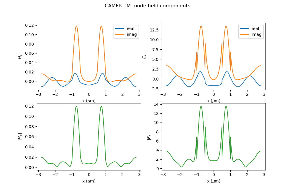
Visualizing the simulation data
Note
CAMFR uses a different coordinate system compared to Ipkiss (Ipkiss x, y, z -> CAMFR z, 1, 2). The latter is being used in the following figure.
num_points = 501
x_positions = np.linspace(0, window_si.height, num_points)
OH2 = np.zeros(len(x_positions), dtype=complex)
OE1 = np.zeros(len(x_positions), dtype=complex)

for x_pos, i in zip(x_positions, range(len(x_positions))):
    coord_output = camfr.Coord(x_pos, 0.0, window_si.width)
    field_output = camfr_stack.field(coord_output)
    OH2[i] = field_output.H2()
    OE1[i] = field_output.E1()

shifted_x_position = x_positions + window_si.south

fig = plt.figure(figsize=(10, 6.5))
fig.suptitle("CAMFR TM mode field components")
plt.subplot(221)
plt.plot(shifted_x_position, OH2.real, "C0", label="real")
plt.plot(shifted_x_position, OH2.imag, "C1", label="imag")
plt.ylabel(r"$H_y$")
plt.xlabel(r"x ($\mu$m)")
plt.legend()

plt.subplot(222)
plt.plot(shifted_x_position, OE1.real, "C0", label="real")
plt.plot(shifted_x_position, OE1.imag, "C1", label="imag")
plt.ylabel(r"$E_x$")
plt.xlabel(r"x ($\mu$m)")
plt.legend()

plt.subplot(223)
plt.plot(shifted_x_position, abs(OH2), "C2", label="abs")
plt.ylabel(r"$|H_y|$")
plt.xlabel(r"x ($\mu$m)")

plt.subplot(224)
plt.plot(shifted_x_position, abs(OE1), "C2", label="abs")
plt.ylabel(r"$|E_x|$")
plt.xlabel(r"x ($\mu$m)")
plt.show()