Note
Go to the end to download the full example code
Netlist Extraction of Multiple layers
This sample illustrates how to extract the complete electrical netlist based on the physical implementation, focusing on the layout with transitions between metal layers through VIAs.
Check i3.NetlistExtractionSettings and get the
complete schematic visualized in IPKISS Canvas.
Importing pdk and library
We start with importing si_fab as PDK technology and pteam_library_si_fab as library
from si_fab import all as pdk
from pteam_library_si_fab import all as lib
from ipkiss3 import all as i3
Creating VIA_M1_M2_ARRAY PCell
For this example, we’ll build a layout with multi-layer connections. The first step is to create a via PCell, VIA_M1_M2_ARRAY PCell, which is based on VIA_M1_M2 in si_fab and will be used throughout this example.
class VIA_M1_M2_ARRAY(i3.PCell):
    box_size = i3.Size2Property(default=(10, 10))
    via_pitch = i3.Size2Property(default=i3.TECH.BONDPAD.VIA_PITCH, doc="(pitch_x, pitch_y) of the vias")
    via = i3.ChildCellProperty(doc="Via cell to be repeated in the array")

    def _default_via(self):
        return pdk.VIA_M1_M2()

    class Layout(i3.LayoutView):
        def _generate_instances(self, insts):
            periods_x = int(self.box_size[0] / self.via_pitch[0]) - 1
            periods_y = int(self.box_size[1] / self.via_pitch[1]) - 1

            insts += i3.ARef(
                reference=self.via,
                origin=(
                    -(periods_x - 1) * self.via_pitch[0] / 2.0,
                    -(periods_y - 1) * self.via_pitch[1] / 2.0,
                ),
                period=self.via_pitch,
                n_o_periods=(periods_x, periods_y),
            )
            return insts

    class Netlist(i3.NetlistFromLayout):
        pass
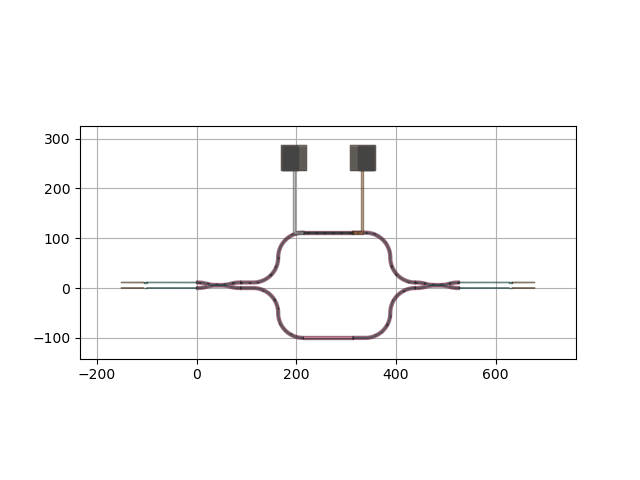
Creating Routed Mach-Zehnder Interferometer
We will create a tunable Mach-Zehnder Interferometer, electrically connected to bondpads through different metal layers, and optically connected to edge couplers. The tunable MZI has already been defined in the programmable photonics circuit tutorial, and is available in the pteam_library_si_fab as PPCUnit.
class RoutedMZI(i3.Circuit):
    bondpad = i3.ChildCellProperty(doc="Bondpad used.")
    ppc_unit = i3.ChildCellProperty(doc="PPC Unit used.")
    via_array = i3.ChildCellProperty(doc="Via_Array used.")
    trace_template = i3.TraceTemplateProperty(doc="trace template of the waveguide port for edge coupler.")
    edge_coupler = i3.ChildCellProperty(doc="Edge coupler used.")

    def _default_edge_coupler(self):
        return pdk.SiNInvertedTaper(trace_template=self.trace_template)

    def _default_via_array(self):
        return VIA_M1_M2_ARRAY(box_size=(4, 4), via_pitch=(1, 1))

    def _default_trace_template(self):
        return pdk.NWG900()

    def _default_bondpad(self):
        return pdk.BondPad()

    def _default_ppc_unit(self):
        return lib.PPCUnit(wg_buffer_dx=25.0, two_arm_length_difference=0.0, bend_radius=50.0)

    def _default_insts(self):
        insts = {
            "bp1": self.bondpad,
            "bp2": self.bondpad,
            "ppc_unit": self.ppc_unit,
            "ec_in1": self.edge_coupler,
            "ec_in2": self.edge_coupler,
            "ec_out1": self.edge_coupler,
            "ec_out2": self.edge_coupler,
        }
        return insts

    def _default_specs(self):
        M1_wire_tpl = pdk.M1WireTemplate().Layout(width=5)
        M2_wire_tpl = pdk.M2WireTemplate().Layout(width=5)

        placement_specs = [
            i3.Place("ppc_unit", (0, 0)),
            i3.PlaceRelative("bp1:m2", "ppc_unit:ht1", (-20, 150)),
            i3.PlaceRelative("bp2:m2", "ppc_unit:ht2", (20, 150)),
        ]

        electrical_connection_specs = [
            i3.ConnectElectrical(
                "ppc_unit:ht1",
                "bp1:m2",
                start_angle=180,
                end_angle=-90,
                end_straight=60,
                trace_template=M1_wire_tpl,
                control_points=[
                    i3.VIA(
                        i3.START,
                        direction_out=i3.WEST,
                        trace_template=M2_wire_tpl,
                        layout=self.via_array,
                    )
                ],
            ),
            i3.ConnectElectrical(
                "ppc_unit:ht2",
                "bp2:m1",
                start_angle=0,
                start_straight=10,
                end_angle=-90,
                end_straight=60,
                trace_template=M1_wire_tpl,
            ),
        ]

        optical_connection_specs = [
            i3.Join("ec_in1:out", "ppc_unit:in1", 0),
            i3.Join("ec_in2:out", "ppc_unit:in2", 0),
            i3.Join("ec_out1:out", "ppc_unit:out1", 180),
            i3.Join("ec_out2:out", "ppc_unit:out2", 180),
        ]

        return placement_specs + electrical_connection_specs + optical_connection_specs

    def _default_exposed_ports(self):
        exposed_ports = {
            "bp1:m1": "bp1_m1",
            "bp2:m2": "bp2_m2",
            "ec_in1:in": "in1",
            "ec_in2:in": "in2",
            "ec_out1:in": "out1",
            "ec_out2:in": "out2",
        }
        return exposed_ports
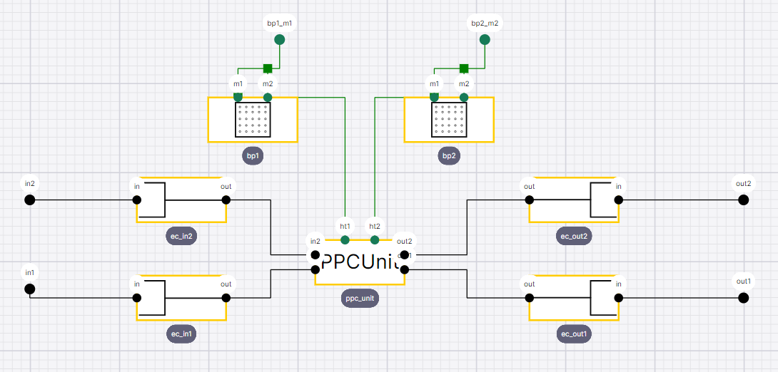
Extracting the netlist
Now let’s have a look at the netlist. This is automatically extracted thanks to
i3.NetlistFromLayout. IPKISS will look at the layout and check for connected
ports, and generate the relevant netlist instances, terms, and optical and single-layer electrical connections.
For the multi-layer connections shown in this sample, we need to manually specify which layers are connected
by using i3.NetlistExtractionSettings and
setting the connected_layers argument. Then we can get the complete schematic visualized
in IPKISS Canvas by to_canvas.
layout = RoutedMZI().Layout()
layout.visualize()

settings = i3.NetlistExtractionSettings(
    electrical=True,
    connected_layers=[
        (i3.TECH.PPLAYER.V12, i3.TECH.PPLAYER.M1),
        (i3.TECH.PPLAYER.V12, i3.TECH.PPLAYER.M2),
    ],
)

layout.to_canvas(project_name="RoutedMZI", netlist_extraction_settings=settings)