ElectricalVia
- class ipkiss3.pcell.via.cell.ElectricalVia
Class for common electrical vias. Its purpose is to electrically connect two layers (
layer_topandlayer_bottom) that are defined in the Layoutview. Two ports/terms namedtopandbottomrefer to the connection points on those respective layers. The connection is done with a connection layer(layer_via)- Parameters:
- name: String that contains only ISO/IEC 8859-1 (extended ASCII py3) or pure ASCII (py2) characters
The unique name of the pcell
Views
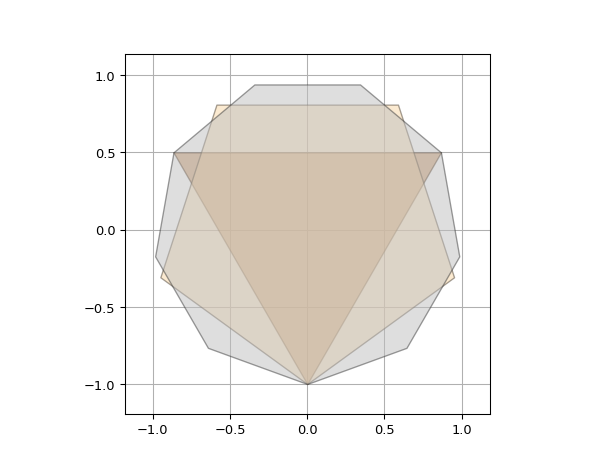
- class Layout
A standard electrical via is made of a boundary on three layers(
layer_top,layer_bottomandlayer_via). For each layer (top,bottomandvia) 2 properties are defined:top_shape
top_layer
analogous properties are defined for the other layers.
- Parameters:
- via_shape: Shape
viashape of the via.- via_layer: Layer
Drawing layer for the
vialayer of the via.- bottom_shape: Shape
Shape used for the
bottomof the via. Also used as shape in thebottomport.- bottom_layer: Layer
Drawing layer for the
bottomof the via.- top_shape: Shape
Shape used for the
topof the via. Also used as shape in thetopport.- top_layer: Layer
Drawing layer for the
topof the via.- view_name: String that contains only alphanumeric characters from the ASCII set or contains _$. ASCII set is extended on PY3.
The name of the view
- Other Parameters:
- layers: locked
- shapes: locked
Examples
import si_fab.all as pdk  # noqa: F401
from ipkiss3 import all as i3
from ipkiss3.pcell.via.cell import ElectricalVia

cell = ElectricalVia()
# defining the shapes that are going to be used
# For the top bottom layer and via layer you can either define a layer or
# a combination of a process and a purpose.

layout = cell.Layout(
    top_shape=i3.ShapeRegularPolygon(n_o_sides=3),
    bottom_shape=i3.ShapeRegularPolygon(n_o_sides=9),
    via_shape=i3.ShapeRegularPolygon(n_o_sides=5),
    top_layer=i3.TECH.PPLAYER.M1.LINE,
    bottom_layer=i3.TECH.PPLAYER.M2.LINE,
    via_layer=i3.TECH.PPLAYER.V12.PILLAR,
)

layout.visualize()