Electrical Components
Electrical wires & components are an important piece of designs. While IPKISS doesn’t replace existing electronics design tools we provide basic functionality to place electrical wires on your design in order to integrate photonics and electrical components effectively.
ElectricalWire
The behavior of ElectricalWire is very similar to that of Waveguide.
- class ipkiss3.all.ElectricalWire
A basic electrical trace ( wire )
- Parameters:
- trace_template: PCell and ElectricalWireTemplate
- external_port_names: str
Dictionary for remapping of the port names of the contents to the external ports
- name: String that contains only ISO/IEC 8859-1 (extended ASCII py3) or pure ASCII (py2) characters
The unique name of the pcell
- Other Parameters:
- contents: PCell and _Trace, locked
Notes
This is a very basic version of an electrical wire, variations exist to suit your more advanced needs
Examples
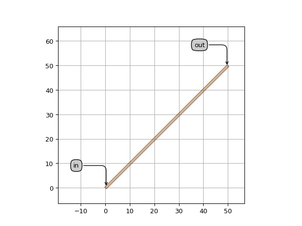
>>> import si_fab.all as pdk
>>> import ipkiss3.all as i3
>>> etpl = i3.ElectricalWireTemplate('my_ewire_tpl')
>>> wire = i3.ElectricalWire(name="my_ewire", trace_template=etpl)
>>> layout = wire.Layout(shape=[(0, 0), (0, 50), (50, 50)])
>>> layout.visualize(annotate=True)
Views
- class Layout
- Parameters:
- trace_template_for_ports: _TraceTemplate.Layout
Trace template to be used for the ports.
- reverse_individual_bends: list<( bool, bool_ or int )>
When set to True, it will generate the individual bends backwards. This has only effect when the bend algorithm is not symmetric. Should have length equal to the shape for closed shapes, but equal to shape-2 for open shapes.
- rounding_algorithms:
Rounding algorithm for every individual bend. Can be circular, spline, … Should have length equal to the shape for closed shapes, but equal to shape-2 for open shapes.
- bend_radii: list<number > 0>
Bend radius for every individual bend.
- reverse_bends: ( bool, bool_ or int )
When set to True, it will generate the bends backwards. This has only effect when the bend algorithm is not symmetric.
- remove_straight_angles: ( bool, bool_ or int )
Removes the waypoints with straight angles. Set to False if the algorithm uses waypoint-specific information.
- shape: Shape
Shape from which the Trace is calculated
- cover_layers: List with type restriction, allowed types: <class ‘ipkiss.primitives.layer.Layer’>
layers that can be used to generate additional coverage of the trace (e.g. manhattan corners)
- control_shape_layer: __Layer__
layer on which the control shape is drawn
- draw_control_shape: ( bool, bool_ or int )
draws the control shape on top of the waveguide
- contents_transformation: GenericNoDistortTransform
- flatten_contents: ( bool, bool_ or int )
if True, it will insert the contents as elements in the layout, rather than as an Instance
- view_name: String that contains only alphanumeric characters from the ASCII set or contains _$. ASCII set is extended on PY3.
The name of the view
- manhattan: ( bool, bool_ or int )
Adds rectangular blocks in the bends to avoid as much as possible non-manhattan angles.
- angle_step: float and number > 0
Angle step for rounding.
- rounding_algorithm:
Rounding algorithm used to generate the bends. Can be circular, spline, ….
- bend_radius: float and number > 0
Bend radius for the auto-generated bends.
- Other Parameters:
- center_line_shape: locked
Automatically calculated shape of the center line of the trace
Examples
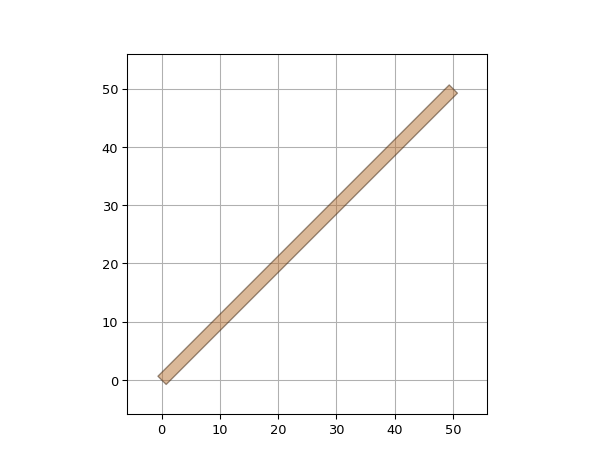
import si_fab.all as pdk  # noqa: F401
import ipkiss3.all as i3

etpl = i3.ElectricalWireTemplate("my_ewire_tpl")
wire = i3.ElectricalWire(name="my_ewire", trace_template=etpl)
layout = wire.Layout(shape=[(0, 0), (50, 50)])
layout.visualize(annotate=True)
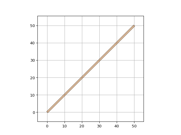
"""Using the electrical wire template you can easily change the
default width of your waveguide"""
import si_fab.all as pdk  # noqa: F401
import ipkiss3.all as i3

etpl = i3.ElectricalWireTemplate("my_thin_ewire_tpl")
etpl.Layout(width=2.0)
wire = i3.ElectricalWire(name="my_thin_ewire", trace_template=etpl)
layout = wire.Layout(shape=[(0, 0), (50, 50)])
layout.visualize()
"""Often you'll just want to use the default ElectricalWireTemplate
specified in the TECH file"""
import si_fab.all as pdk  # noqa: F401
import ipkiss3.all as i3

wire = i3.ElectricalWire(name="my_thin_ewire", trace_template=i3.TECH.PCELLS.METAL.DEFAULT)
layout = wire.Layout(shape=[(0, 0), (50, 50)])
layout.visualize()
- class Netlist
- Parameters:
- trace_template_for_terms: _TraceTemplate.Netlist
Trace template to be used for the terms.
- view_name: String that contains only alphanumeric characters from the ASCII set or contains _$. ASCII set is extended on PY3.
The name of the view
Examples
"""Netlists of an electrical wire are most of the time very simple.
Though it's important to remark that all terms will be connected to 1 net"""

import si_fab.all as pdk  # noqa: F401
import ipkiss3.all as i3

wire = i3.ElectricalWire(name="my_wire_withnetlist")
netlist = wire.Netlist()

nets = netlist.nets

# The electrical wire only contains 1 net
assert len(nets) == 1

# And this nets contains all the given terms
assert nets[0].terms == list(netlist.terms.values())

# Let's print the terms
print(netlist.terms)
ElectricalWireTemplate
TraceTemplate used to create electrical wires.
- class ipkiss3.all.ElectricalWireTemplate
A TraceTemplate to easily create electrical wires
- Parameters:
- name: String that contains only ISO/IEC 8859-1 (extended ASCII py3) or pure ASCII (py2) characters
The unique name of the pcell
Views
- class Layout
- Parameters:
- layer: __Layer__
- pin_shape: Shape
shape to be used for the pins
- trace_template_for_ports: _TraceTemplate.Layout
Trace template to be used for the ports. Default = this template
- control_shape_layer: __Layer__
layer on which the control shape is drawn
- draw_control_shape: ( bool, bool_ or int )
draws the control shape on top of the waveguide
- width: float and number > 0
Width of the electrical trace
- view_name: String that contains only alphanumeric characters from the ASCII set or contains _$. ASCII set is extended on PY3.
The name of the view
- class Netlist
- Parameters:
- trace_template_for_terms: _TraceTemplate.Netlist
Trace template to be used for the terms. Default = this template
- view_name: String that contains only alphanumeric characters from the ASCII set or contains _$. ASCII set is extended on PY3.
The name of the view
ElectricalWindowWireTemplate
As with waveguides you can create new templates for your electrical wires. This way you can build more custom & specialized wires.
- class ipkiss3.all.ElectricalWindowWireTemplate
An advanced trace template that is used to define electrical wires using ‘windows’. These windows will be extruded extruded along the shape of the wire
- Parameters:
- name: String that contains only ISO/IEC 8859-1 (extended ASCII py3) or pure ASCII (py2) characters
The unique name of the pcell
See also
Notes
This trace template is only useful in more advanced usecases. When you want to create simple wires, ElectricalWireTemplate should be sufficient.
Views
- class Layout
- Parameters:
- windows: List with type restriction, allowed types: <class ‘ipkiss3.pcell.trace.window.window._TraceWindow’>
List of Trace Windows that know how to draw themselves relative to the shape of the Trace
- layer: __Layer__
- pin_shape: Shape
shape to be used for the pins
- trace_template_for_ports: _TraceTemplate.Layout
Trace template to be used for the ports. Default = this template
- control_shape_layer: __Layer__
layer on which the control shape is drawn
- draw_control_shape: ( bool, bool_ or int )
draws the control shape on top of the waveguide
- width: float and number > 0
Width of the electrical trace
- view_name: String that contains only alphanumeric characters from the ASCII set or contains _$. ASCII set is extended on PY3.
The name of the view
Examples
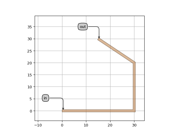
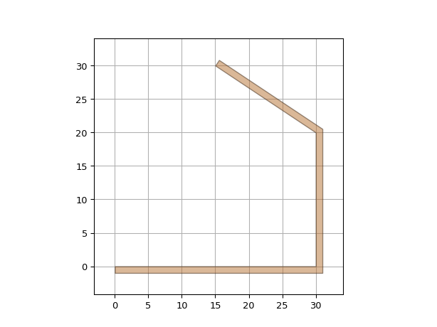
import si_fab.all as pdk  # noqa: F401
import ipkiss3.all as i3

etpl = i3.ElectricalWindowWireTemplate()
etpl.Layout()
wire = i3.ElectricalWire(name="my_wire_with_windows", trace_template=etpl)
layout = wire.Layout(shape=[(0.0, 0.0), (30.0, 0.0), (30.0, 20.0), (15.0, 30.0)])
layout.visualize(annotate=True)
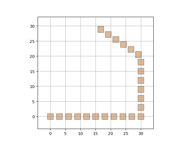
"""Windows provide you the possiblity to create more
advanced wires"""
import si_fab.all as pdk  # noqa: F401
import ipkiss3.all as i3

etpl = i3.ElectricalWindowWireTemplate()

metal_layer = i3.PPLayer(process=i3.TECH.METAL.DEFAULT_PROCESS, purpose=i3.TECH.PURPOSE.DF.LINE)

windows = [i3.PathTraceWindow(layer=metal_layer, start_offset=-1, end_offset=0)]

etpl.Layout(draw_control_shape=True, windows=windows)

wire = i3.ElectricalWire(name="my_wire_with_windows2", trace_template=etpl)
layout = wire.Layout(shape=[(0.0, 0.0), (30.0, 0.0), (30.0, 20.0), (15.0, 30.0)])
layout.visualize()
"""A toy example that uses PeriodicReferenceTraceWindow"""
import si_fab.all as pdk  # noqa: F401
import ipkiss3.all as i3
from ipkiss3.pcell.trace.window.reference_window import PeriodicReferenceTraceWindow
from ipkiss.process import PPLayer

metal_layer = PPLayer(process=i3.TECH.METAL.DEFAULT_PROCESS, purpose=i3.TECH.PURPOSE.DF.LINE)

class MyCell(i3.PCell):
    class Layout(i3.LayoutView):
        def _generate_elements(self, elems):
            elems += i3.Rectangle(layer=metal_layer, box_size=(2.0, 2.0))
            return elems

my_layout = MyCell().Layout()

etpl = i3.ElectricalWindowWireTemplate()

windows = [PeriodicReferenceTraceWindow(reference=my_layout, pitch=3.0)]

etpl.Layout(windows=windows)

wire = i3.ElectricalWire(name="my_crazy_ewire", trace_template=etpl)
layout = wire.Layout(shape=[(0.0, 0.0), (30.0, 0.0), (30.0, 20.0), (15.0, 30.0)])
layout.visualize()
- class Netlist
- Parameters:
- trace_template_for_terms: _TraceTemplate.Netlist
Trace template to be used for the terms. Default = this template
- view_name: String that contains only alphanumeric characters from the ASCII set or contains _$. ASCII set is extended on PY3.
The name of the view
Electrical Vias
Vias are components that connect a metal layer with another one that is above or below it using via shapes. Those shapes are also used in the electrical ports in the via. IPKISS only contains base classes for vias should you want to make your own.
Class for common electrical vias. |
|
Most generic class for electrical vias. |