Picazzo Reference (single-page)
This a alternative to the picazzo reference. Instead of offering the reference as seperate pages, this reference combines all information in 1 webpage. This results in a very big page, but the advantage is that it’s easily searchable/navigatable.
Logical Blocks
Coupler1x2
- class picazzo3.logical.coupler.cell.Coupler1x2
A logical 1x2 reciprocal waveguide coupler.
Transmissions and reflections and backcoupling can be set using the properties to arbitrary values without any enforcement of passivity.
Properties dealing with transmission: straight_coupling1, straight_coupling2 Properties dealing with reflection: reflection_in1, reflection_out1, reflection_out2 Properties dealing with back coupling: back_coupling
The default behaviour of the coupler model assumes symmetry that allows the permutations (out_1 with out_2) in the first place. If your component uses this symmetry, properties only have to be specified for in and out_1, the ones relating to out_2 will be assuming this symmetry.
In the second place the coupler model assumes symmetry that allows the permutation of output ports with input ports.
- Parameters:
- name: String that contains only ISO/IEC 8859-1 (extended ASCII py3) or pure ASCII (py2) characters
The unique name of the pcell
- Other Parameters:
- n_outputs: int and number > 0, locked
Number of output channels.
- n_inputs: int and number > 0, locked
Number of input channels.
Coupler2x1
- class picazzo3.logical.coupler.cell.Coupler2x1
A logical 2x1 reciprocal waveguide coupler.
Transmissions and reflections and backcoupling can be set using the properties to arbitrary values without any enforcement of passivity.
Properties dealing with transmission: straight_coupling1, straight_coupling2 Properties dealing with reflection: reflection_out1, reflection_in1, reflection_in2 Properties dealing with back coupling: back_coupling
The default behaviour of the coupler model assumes symmetry that allows the permutations (in1 with in2) in the first place. If your component uses this symmetry, properties only have to be specified for in1 and out, the ones relating to in2 will be assuming this symmetry.
In the second place the coupler model assumes symmetry that allows the permutation of output ports with input ports.
- Parameters:
- name: String that contains only ISO/IEC 8859-1 (extended ASCII py3) or pure ASCII (py2) characters
The unique name of the pcell
- Other Parameters:
- n_outputs: int and number > 0, locked
Number of output channels.
- n_inputs: int and number > 0, locked
Number of input channels.
Coupler2x2
- class picazzo3.logical.coupler.cell.Coupler2x2
A logical 2x2 reciprocal waveguide coupler.
Transmissions and reflections and backcoupling can be set using the properties to arbitrary values without any enforcement of passivity.
Properties dealing with transmission: cross_coupling1, cross_coupling2, straight_coupling1, straight_coupling2 Properties dealing with reflection: reflection_in1, reflection_in2, reflection_out1, reflection_out2 Properties dealing with back coupling: back_coupling_in, back_coupling_out
The default behaviour of the coupler model assumes symmetry that allows the permutations (in_1 with in_2) and (out_1 with out_2) in the first place. If your component uses this symmetry, properties only have to be specified for in_1 and out_1, the ones relating to in_2 and out_2 will be assuming this symmetry.
In the second place the coupler model assumes symmetry that allows the permutation of output ports with input ports.
- Parameters:
- name: String that contains only ISO/IEC 8859-1 (extended ASCII py3) or pure ASCII (py2) characters
The unique name of the pcell
- Other Parameters:
- n_outputs: int and number > 0, locked
Number of output channels.
- n_inputs: int and number > 0, locked
Number of input channels.
Reflector
- class picazzo3.logical.reflector.cell.Reflector
Logical reflector: reflects a part of the light and passes on the rest
- Parameters:
- name: String that contains only ISO/IEC 8859-1 (extended ASCII py3) or pure ASCII (py2) characters
The unique name of the pcell
WaveguideReflector
- class picazzo3.logical.reflector.cell.WaveguideReflector
Zero-length waveguide reflector: calculates reflection based on the waveguide templates
- Parameters:
- wg_template_out: PCell and _WaveguideTemplate
Waveguide template at the output
- wg_template_in: PCell and _WaveguideTemplate
Waveguide template at the input
- name: String that contains only ISO/IEC 8859-1 (extended ASCII py3) or pure ASCII (py2) characters
The unique name of the pcell
Termination
- class picazzo3.logical.termination.cell.Termination
Logical component: a termination Has one input, no outputs. A reflectivity can be specified but defaults to 0.0 Use this to terminate terminals of PCells to avoid reflections and unconnected terms
- Parameters:
- name: String that contains only ISO/IEC 8859-1 (extended ASCII py3) or pure ASCII (py2) characters
The unique name of the pcell
PerfectTermination
- class picazzo3.logical.termination.cell.PerfectTermination
Logical component: a perfect termination Has one input, no outputs and does not reflect any signal. Use this to terminate terminals of PCells to avoid reflections and unconnected terms
- Parameters:
- name: String that contains only ISO/IEC 8859-1 (extended ASCII py3) or pure ASCII (py2) characters
The unique name of the pcell
Grating Couplers
FiberCouplerCurvedGrating
- class picazzo3.fibcoup.curved.cell.FiberCouplerCurvedGrating
Class for the definition of periodic curved fiber grating couplers with a focal point that fit in a box.
- Parameters:
- inclination: float
out-of-plane angle of the grating coupler
- grating: PCell
grating of this fiber coupler
- wide_trace_template: PCell and _WaveguideTemplate
end waveguide for the socket waveguide (broad side)
- start_trace_template: PCell and _WaveguideTemplate
start waveguide for the socket waveguide (narrow side)
- socket: PCell and WgSocket
socket of the fiber coupler
- name: String that contains only ISO/IEC 8859-1 (extended ASCII py3) or pure ASCII (py2) characters
The unique name of the pcell
Views
- class Layout
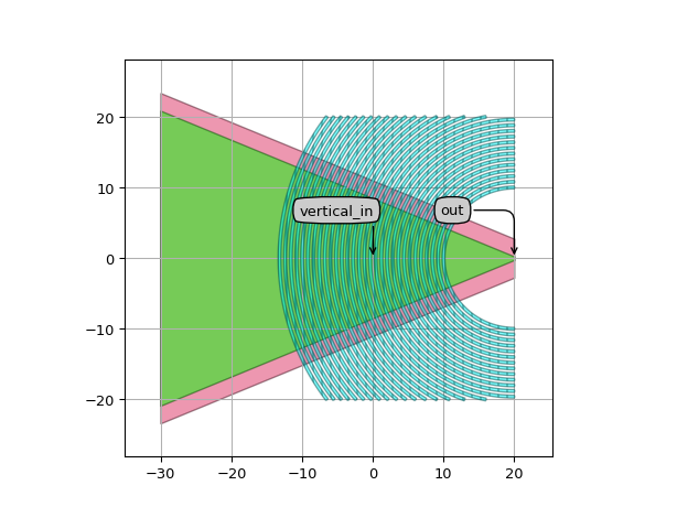
This class generates a fiber grating coupler composed of a curved fiber grating with a LinearTransitionSocket. The origin of the coordinate system of the component is placed where the center of the fiber facet is assumed to have maximal coupling efficiency. This also the location of the vertical port
vertical_in.The grating lines generated by this class have the following properties.
1. All the grating lines have a shared focus point that is the east focus point of all the ellipses. The focus point has to be on the x-axis. The location of the focus is set by
focal_distance_xand will be located east of the origin.2. The first grating line will be drawn a distance
min_xfrom the focus point. So ifmin_x = 10, this means that the distance between the focus point and the first grating line will exactly be 10. By default, min_x is set to:3. All the grating lines are periodic in the x-direction with
period_x. This means that the distance between the intersections of grating lines with the x-axis is equal toperiod_x.4. All the grating lines are periodic in the y direction with
period_y. This means that the distance between the intersections grating lines with the y-axis is equal toperiod_y.The radius of the first ellipse in the y-direction is set be
start_radius_y.The radius of the first ellipse in the x-direction is automatically calculated and therefore locked.
7. All the grating lines fit in a box with width set by
box_widththat is symmetrically set along the x-axis. For example ifbox_widthis set to 10.0 all the grating lines will go fromy=-5.0toy=5.0.8. The width of all the grating lines is set by
fill_factor. A fill factor of 1 makes that the line width is a wide as the period. A fill factor of 0 makes sets the line_width to 0.The socket is a LinearTransitionSocket transitioning from the
start_trace_templatetowide_trace_template.start_trace_templateis the template seen at the focal point whilewide_trace_templateis the one seen at the location of the vertical port ``vertical_in`. The length of the transitionsocket_lengthis therefore locked and automatically set to thefocal_distance_x.To extend the taper beyond the focal point you can use the property
socket_extensionwhich will automatically prolong the taper with the lengthsocket_extensionThe default value ofextensionis chosen such that entire grating fits in the socket.- Parameters:
- fill_factor: float and fraction
Fill factor used to calculate the trench widths. 0 means no trench a all and 1 means that the trench covers the entire period
- purpose:
- process: ProcessLayer
default process used for the grating
- grating_transformation: GenericNoDistortTransform
transformation of the grating in this fiber coupler cell
- spread_angle: float
Angle in degrees of the far field radiation field of the socket.By default this is set to be equal to the angle of the taper that is set by its length and the width of the core of input and output waveguides.
- period_x: float and number > 0
Period in the x direction.
- min_x: float and number > 0
Minimum distance from the first line to the focus. By default it is set to the focal distance.
- focal_distance_x: float
Distance between the vertical port of the grating and the focal point. By default this is TECH.IO.FIBCOUP.CURVED.GRATING.FOCAL_DISTANCE.
- start_radius_y: float and number > 0
Starting radius in the y direction. By default this is set to
start_period_x- period_y: float and number > 0
Period in the y direction. By default equal to
period_x- box_width: float and number > 0
Width of the box used that contains the grating.
- n_o_lines: int and number > 0
Number of lines in the grating. By default this number is chosen so that the curves fit in the box width.
- socket_straight_extension: Coord2 and number >= 0
tuple: straight extension at start and end of socket
- socket_extension: float and Real, number and number >= 0
extension of the wide side of the socket, asymmetric with respect to the specified center. By default this is calculated such that the entire grating fits in the socket with a margin of TECH.IO.FIBCOUP.CURVED.DEFAULT_SOCKET_MARGIN_FROM_GRATING
- socket_transformation: GenericNoDistortTransform
transformation of the socket in the fiber coupler
- view_name: String that contains only alphanumeric characters from the ASCII set or contains _$. ASCII set is extended on PY3.
The name of the view
- Other Parameters:
- ellipse_radii_y: locked
- ellipse_radii_x: locked
- centers: locked
- focal_point: Coord2, locked
Coordinate of the east focus point shared by all ellipses. The y coordinate of the focuspoint has to be zero
- start_radius_x: locked
- line_widths: locked
Line width of the grating coupler
- end_angles: locked
- start_angles: locked
- socket_length: locked
Examples
Basic use:
# Example demonstrating the basic use of the FiberGratingCoupler.
import si_fab.all as pdk  # noqa: F401
from ipkiss3 import all as i3

from picazzo3.fibcoup.curved import FiberCouplerCurvedGrating
from picazzo3.traces.wire_wg import WireWaveguideTemplate

# Creating the wire templates for the socket.
start_wg_tmpl = WireWaveguideTemplate()
start_wg_tmpl.Layout(core_width=0.5, cladding_width=2 * i3.TECH.WG.TRENCH_WIDTH + 0.5)
end_wg_tmpl = WireWaveguideTemplate()
end_wg_tmpl.Layout(core_width=17.0, cladding_width=2 * i3.TECH.WG.TRENCH_WIDTH + 17.0)

fc_cell = FiberCouplerCurvedGrating(start_trace_template=start_wg_tmpl, wide_trace_template=end_wg_tmpl)

fc_layout = fc_cell.Layout(
    period_x=0.8, focal_distance_x=20.0  # We with a period of 0.8
)  # We use a focal distance of 20.0

fc_layout.visualize(annotate=True)
Changing the
n_o_linesand where to place the first line:# Example demonstrating how to change the length of the grating coupler using n_o_lines # and how to set the location of the first grating line using min_x import si_fab.all as pdk # noqa: F401 from ipkiss3 import all as i3 from picazzo3.fibcoup.curved import FiberCouplerCurvedGrating from picazzo3.traces.wire_wg import WireWaveguideTemplate # Creating the wire templates for the socket. start_wg_tmpl = WireWaveguideTemplate() start_wg_tmpl.Layout(core_width=0.5, cladding_width=2 * i3.TECH.WG.TRENCH_WIDTH + 0.5) end_wg_tmpl = WireWaveguideTemplate() end_wg_tmpl.Layout(core_width=17.0, cladding_width=2 * i3.TECH.WG.TRENCH_WIDTH + 17.0) fc_cell = FiberCouplerCurvedGrating(start_trace_template=start_wg_tmpl, wide_trace_template=end_wg_tmpl) fc_layout = fc_cell.Layout( period_x=0.8, # We with a period of 0.8 focal_distance_x=20.0, # We use a focal distance of 20.0 n_o_lines=30, # We set the number of lines to 30 min_x=10.0, # We set the first line at 10. ) fc_layout.visualize(annotate=True)

Changing the
box_width:# Example demonstrating how to change the box_width. import si_fab.all as pdk # noqa: F401 from ipkiss3 import all as i3 from picazzo3.fibcoup.curved import FiberCouplerCurvedGrating from picazzo3.traces.wire_wg import WireWaveguideTemplate # Creating the wire templates for the socket. start_wg_tmpl = WireWaveguideTemplate() start_wg_tmpl.Layout(core_width=0.5, cladding_width=2 * i3.TECH.WG.TRENCH_WIDTH + 0.5) end_wg_tmpl = WireWaveguideTemplate() end_wg_tmpl.Layout(core_width=17.0, cladding_width=2 * i3.TECH.WG.TRENCH_WIDTH + 17.0) fc_cell = FiberCouplerCurvedGrating(start_trace_template=start_wg_tmpl, wide_trace_template=end_wg_tmpl) fc_layout = fc_cell.Layout( period_x=0.8, # We with a period of 0.8 focal_distance_x=20.0, # We use a focal distance of 20.0. n_o_lines=30, # We set the number of lines to 30. min_x=10.0, # We set the first line at 10. box_width=40.0, # All the lines will be contained between -20 and 20 ) fc_layout.visualize(annotate=True)
Changing the
fill_factorto set the line width:# Example demonstrating how to change the fill_factor. import si_fab.all as pdk # noqa: F401 from ipkiss3 import all as i3 from picazzo3.fibcoup.curved import FiberCouplerCurvedGrating from picazzo3.traces.wire_wg import WireWaveguideTemplate # Creating the wire templates for the socket. start_wg_tmpl = WireWaveguideTemplate() start_wg_tmpl.Layout(core_width=0.5, cladding_width=2 * i3.TECH.WG.TRENCH_WIDTH + 0.5) end_wg_tmpl = WireWaveguideTemplate() end_wg_tmpl.Layout(core_width=17.0, cladding_width=2 * i3.TECH.WG.TRENCH_WIDTH + 17.0) fc_cell = FiberCouplerCurvedGrating(start_trace_template=start_wg_tmpl, wide_trace_template=end_wg_tmpl) fc_layout = fc_cell.Layout( period_x=0.8, # We with a period of 0.8 focal_distance_x=20.0, # We use a focal distance of 20.0. n_o_lines=30, # We set the number of lines to 30. min_x=10.0, # We set the first line at 10. fill_factor=0.2, # Here we set the fill factor to 0.2 meaning that lines will be 0.2 * period_x thick ) fc_layout.visualize(annotate=True)
Changing the start radii in the y direction:
# Example that illustrates the degrees of freedom at your disposal concerning the
# periodicity and radii of the gratings in the y direction. You have more freedom in
# y direction since the focus is in the x-axis.

import si_fab.all as pdk  # noqa: F401
from ipkiss3 import all as i3

from picazzo3.fibcoup.curved import FiberCouplerCurvedGrating
from picazzo3.traces.wire_wg import WireWaveguideTemplate

# Creating the wire templates for the socket.
start_wg_tmpl = WireWaveguideTemplate()
start_wg_tmpl.Layout(core_width=0.5, cladding_width=2 * i3.TECH.WG.TRENCH_WIDTH + 0.5)
end_wg_tmpl = WireWaveguideTemplate()
end_wg_tmpl.Layout(core_width=17.0, cladding_width=2 * i3.TECH.WG.TRENCH_WIDTH + 17.0)

fc_cell = FiberCouplerCurvedGrating(start_trace_template=start_wg_tmpl, wide_trace_template=end_wg_tmpl)

fc_layout = fc_cell.Layout(
    focal_distance_x=20.0,  # We use a focal distance of 20.0.
    n_o_lines=30,  # We use 30 lines.
    period_x=0.8,  # We with a period of 0.8
    period_y=0.5,  # period has to be smaller than the period in the x direction
    start_radius_y=3.0,  # Start_radius_y has to be smaller than min_x
    fill_factor=0.2,  # Fill factor of 0.2
    min_x=10.0,  # First line at 10.0
)

fc_layout.visualize(annotate=True)

Changing the socket extensions:
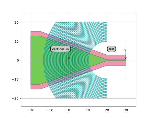
# Example demonstrating how to change the socket_extension.
import si_fab.all as pdk  # noqa: F401
from ipkiss3 import all as i3

from picazzo3.fibcoup.curved import FiberCouplerCurvedGrating
from picazzo3.traces.wire_wg import WireWaveguideTemplate

# Creating the wire templates for the socket.
start_wg_tmpl = WireWaveguideTemplate()
start_wg_tmpl.Layout(core_width=0.5, cladding_width=2 * i3.TECH.WG.TRENCH_WIDTH + 0.5)
end_wg_tmpl = WireWaveguideTemplate()
end_wg_tmpl.Layout(core_width=17.0, cladding_width=2 * i3.TECH.WG.TRENCH_WIDTH + 17.0)

fc_cell = FiberCouplerCurvedGrating(start_trace_template=start_wg_tmpl, wide_trace_template=end_wg_tmpl)

fc_layout = fc_cell.Layout(
    period_x=0.8,  # We with a period of 0.8
    focal_distance_x=20.0,  # We use a focal distance of 20.0.
    n_o_lines=30,  # We set the number of lines to 30.
    min_x=10.0,  # We set the first line at 10.
    box_width=40.0,  # All the lines will be contained between -20 and 20
    socket_extension=30.0,  # A socket extension will of 30.0 will be added
)

fc_layout.visualize(annotate=True)
Changing the straight socket extensions:
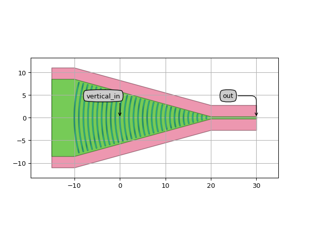
# Example demonstrating how to change the socket_straight_extensions.
import si_fab.all as pdk  # noqa: F401
from ipkiss3 import all as i3

from picazzo3.fibcoup.curved import FiberCouplerCurvedGrating
from picazzo3.traces.wire_wg import WireWaveguideTemplate

# Creating the wire templates for the socket.
start_wg_tmpl = WireWaveguideTemplate()
start_wg_tmpl.Layout(core_width=0.5, cladding_width=2 * i3.TECH.WG.TRENCH_WIDTH + 0.5)
end_wg_tmpl = WireWaveguideTemplate()
end_wg_tmpl.Layout(core_width=17.0, cladding_width=2 * i3.TECH.WG.TRENCH_WIDTH + 17.0)

fc_cell = FiberCouplerCurvedGrating(start_trace_template=start_wg_tmpl, wide_trace_template=end_wg_tmpl)

fc_layout = fc_cell.Layout(
    period_x=0.8,  # We with a period of 0.8
    focal_distance_x=20.0,  # We use a focal distance of 20.0.
    n_o_lines=30,  # We set the number of lines to 30.
    min_x=10.0,  # We set the first line at 10.
    box_width=40.0,
    # A straight extension of 10.0 will be added at the
    # narrow side and 5.0 at the wide part of the socket.
    socket_straight_extension=(10.0, 5.0),
)

fc_layout.visualize(annotate=True)
FiberCouplerCurvedGratingGeneric
- class picazzo3.fibcoup.curved.cell.FiberCouplerCurvedGratingGeneric
Class allowing the creating of generic fiber curved grating coupler. This class allows you to define each grating line individually as long as the grating lines themselves are ellipses.
- Parameters:
- inclination: float
out-of-plane angle of the grating coupler
- grating: PCell
grating of this fiber coupler
- wide_trace_template: PCell and _WaveguideTemplate
end waveguide for the socket waveguide (broad side)
- start_trace_template: PCell and _WaveguideTemplate
start waveguide for the socket waveguide (narrow side)
- socket: PCell and WgSocket
socket of the fiber coupler
- name: String that contains only ISO/IEC 8859-1 (extended ASCII py3) or pure ASCII (py2) characters
The unique name of the pcell
Views
- class Layout
When using this class you have to specify
centers,ellipse_radii_x,ellipse_radii_y,start_angles,end_angles,line_widthsas a list of numbers. A fiber grating coupler composed of ellipses using those parameters will be constructed on a LinearTransitionSocket.It is advised (but not strictly required) to place the intended location of the fiber in the origin of your component. To make sure that this the case you can use
socket_transformationandgrating_transformationto independently transform both the socket and the grating.You can also add extensions to your socket by using the property
socket_straight_extension.- Parameters:
- ellipse_radii_y: list
List of y radii of the ellipses. By default identical to
ellipse_radii_y- ellipse_radii_x: list
List of x radii of the ellipses. By default a list of radii matching the number of center and a period of TECH.IO.FIBCOUP.CURVED.GRATING.PERIOD
- centers: list and List with type restriction, allowed types: <class ‘ipkiss.geometry.coord.Coord2’>
List of centers for the ellipses. By default [i3.Coord2(0, 0)] * TECH.IO.FIBCOUP.CURVED.GRATING.N_O_LINES
- purpose:
- process: ProcessLayer
default process used for the grating
- grating_transformation: GenericNoDistortTransform
transformation of the grating in this fiber coupler cell
- spread_angle: float
Angle in degrees of the far field radiation field of the socket.By default this is set to be equal to the angle of the taper that is set by its length and the width of the core of input and output waveguides.
- line_widths: list
List of the linewidth of the trench of each ellipse. By default TECH.IO.FIBCOUP.CURVED.GRATING.PERIOD / 2.0 for all lines
- end_angles: list
List of the end angle for each ellipse. By default 360 -
start_angles- start_angles: list
List of the start angle in degrees for each ellipse. By default 180 - TECH.FIBCOUP.DEFAULT_ANGLE_SPAN / 2.0 for all lines
- socket_straight_extension: Coord2 and number >= 0
tuple: straight extension at start and end of socket
- socket_extension: float and Real, number and number >= 0
extension of the wide side of the socket, asymmetric with respect to the specified center
- socket_length: float and number > 0
length of the straight waveguide socket
- socket_transformation: GenericNoDistortTransform
transformation of the socket in the fiber coupler
- view_name: String that contains only alphanumeric characters from the ASCII set or contains _$. ASCII set is extended on PY3.
The name of the view
- Other Parameters:
- n_o_lines: int and number > 0, locked
Number of trenches.
Examples
import si_fab.all as pdk  # noqa: F401
from ipkiss3 import all as i3

from picazzo3.fibcoup.curved import FiberCouplerCurvedGratingGeneric
from picazzo3.traces.wire_wg import WireWaveguideTemplate

# Creating the wire templates for the socket.
start_wg_tmpl = WireWaveguideTemplate()
start_wg_tmpl.Layout(core_width=0.5, cladding_width=2 * i3.TECH.WG.TRENCH_WIDTH + 0.5)
end_wg_tmpl = WireWaveguideTemplate()
end_wg_tmpl.Layout(core_width=17.0, cladding_width=2 * i3.TECH.WG.TRENCH_WIDTH + 17.0)

fc_cell = FiberCouplerCurvedGratingGeneric(
    start_trace_template=start_wg_tmpl, wide_trace_template=end_wg_tmpl
)

fc_layout = fc_cell.Layout(
    centers=[i3.Coord2(0, 0) for _ in range(30)],
    ellipse_radii_x=[i + 1 for i in range(30)],
    ellipse_radii_y=[i + 0.9 for i in range(30)],
    start_angles=[180.0 - 15 for _ in range(30)],
    end_angles=[180.0 + 15 for _ in range(30)],
    line_widths=[0.2 for _ in range(30)],
    socket_length=30,
    socket_transformation=i3.Translation(translation=(-10.0, 0.0)),
    grating_transformation=i3.Translation(translation=(20, 0)),
    socket_straight_extension=(10.0, 5.0),
)

fc_layout.visualize(annotate=True)
UniformLineGrating
- class picazzo3.fibcoup.uniform.cell.UniformLineGrating
Uniform 1D fiber coupler grating consisting of identical grating lines, on a straight waveguide socket
- Parameters:
- inclination: float
out-of-plane angle of the grating coupler
- grating: PCell
grating of this fiber coupler
- trace_template: PCell and _TraceTemplate
trace template for the socket waveguide
- socket: PCell and WgSocket
socket of the fiber coupler
- name: String that contains only ISO/IEC 8859-1 (extended ASCII py3) or pure ASCII (py2) characters
The unique name of the pcell
Views
- class Layout
- Parameters:
- n_o_periods: int and number > 0
number of periods of the grating
- origin: Coord2
local origin of the grating (first trench)
- period: float and number > 0
period of the grating
- purpose: PatternPurpose
drawing purpose for the grating lines
- process: ProcessLayer
process layer for the grating
- line_length: float and number > 0
length of the grating trenches (perpendicular to the socket waveguide)
- line_width: float and number > 0
width of the grating trenches, drawn in the given layer
- grating_transformation: GenericNoDistortTransform
transformation of the grating in this fiber coupler cell
- socket_length: float and number > 0
length of the straight waveguide socket
- socket_transformation: GenericNoDistortTransform
transformation of the socket in the fiber coupler
- view_name: String that contains only alphanumeric characters from the ASCII set or contains _$. ASCII set is extended on PY3.
The name of the view
Examples
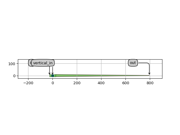
# Creation of a uniform grating coupler with a taper.
import si_fab.all as pdk  # noqa: F401
from picazzo3.traces.wire_wg import WireWaveguideTemplate
from picazzo3.fibcoup.uniform import UniformLineGrating

# Creating the trace template for the grating area
wg_coupler = WireWaveguideTemplate()
wg_coupler.Layout(core_width=15.0, cladding_width=18.0)

FGC = UniformLineGrating(trace_template=wg_coupler)
FGC.Layout(period=0.8, line_width=0.4, line_length=18.0, n_o_periods=24)

# Adding taper to the fibergrating coupler.

# trace template for the connecting waveguide.
wg_t = WireWaveguideTemplate()
wg_t.Layout(core_width=0.5, cladding_width=4.0)

from picazzo3.container.transition_ports import AutoTransitionPorts

Tapered_FCG = AutoTransitionPorts(contents=FGC, port_labels=["out"], trace_template=wg_t)
Tapered_FCG.Layout().visualize(annotate=True)
FiberCouplerGrating
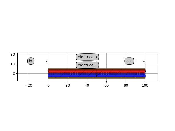
- class picazzo3.fibcoup.base.FiberCouplerGrating
Base class for fiber couplers which combine a grating on top of a socket.
The socket is the piece of waveguide, taper or slab on which the grating rests. The grating couples light between the plane (the socket) and the out-of-plane direction, to a fiber, lens or free space.
This cell should be used such that the inclination and angle of the port match the direction of peak transmission at the center wavelength specified in the circuitmodel, when light is incident from the vertical (through vertical_in) and couples to the out port
             *  "vertical_in"
              *
               *
inclination   / *
            _/  _*  _   _
     "in" _| |_| |_| |_| |_  ---> "out"
- Parameters:
- grating: PCell
grating of this fiber coupler
- inclination: float
out-of-plane angle of the grating coupler
- socket: PCell and WgSocket
socket of the fiber coupler
- name: String that contains only ISO/IEC 8859-1 (extended ASCII py3) or pure ASCII (py2) characters
The unique name of the pcell
Views
- class Layout
- Parameters:
- grating_transformation: GenericNoDistortTransform
transformation of the grating in this fiber coupler cell
- socket_length: float and number > 0
length of the straight waveguide socket
- socket_transformation: GenericNoDistortTransform
transformation of the socket in the fiber coupler
- view_name: String that contains only alphanumeric characters from the ASCII set or contains _$. ASCII set is extended on PY3.
The name of the view
Filters
Ringresonators
RingRect
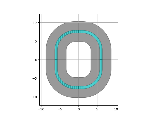
- class picazzo3.filters.ring.cell.RingRect
A Ring resonator consisting of a rounded rectangular trace.
You should specify the trace template for the ring and a shape
By default, this ring has no couplers. you can supply the couplers manually as a list of child cells through the property ‘couplers’, or you can subclass this PCell to define the couplers internally.
- Parameters:
- ring_trace_template: PCell and _WaveguideTemplate
Trace template for the ring waveguide
- ring_segments: List with type restriction, allowed types: <class ‘ipkiss3.pcell.cell.pcell.PCell’>
list of Ring PCells
- couplers: List with type restriction, allowed types: <class ‘ipkiss3.pcell.cell.pcell.PCell’>
list of coupler PCells
- name: String that contains only ISO/IEC 8859-1 (extended ASCII py3) or pure ASCII (py2) characters
The unique name of the pcell
- Other Parameters:
- ring_trace_templates: List with type restriction, allowed types: <class ‘ipkiss3.pcell.cell.pcell.PCell’>, locked
Trace templates for the ring segments. Locked, as there is only one segment in this Ring. Use ‘ring_trace_template’ instead.
See also
Views
- class Layout
- Parameters:
- straights: Coord2 and number >= 0
- shape_position: Coord2
Translation of the shape.
- coupler_transformations:
list of coupler transformations
- area_layer_on: ( bool, bool_ or int )
When True, the Ring area will be covered by i3.Rectangles on all cover layers of the ring waveguide template.
- coupler_parameters:
Parameters for the couplers. This is a list of dicts, and the length of the list should be the same as the number of couplers
- view_name: String that contains only alphanumeric characters from the ASCII set or contains _$. ASCII set is extended on PY3.
The name of the view
- manhattan: ( bool, bool_ or int )
Adds rectangular blocks in the bends to avoid as much as possible non-manhattan angles.
- angle_step: float and number > 0
Angle step for rounding.
- rounding_algorithm:
Rounding algorithm used to generate the bends. Can be circular, spline, ….
- bend_radius: float and number > 0
Bend radius for the auto-generated bends.
- Other Parameters:
- shape: locked
- shapes: locked
Shapes of the ring segments. Locked, as there is only 1 ring segment. Use ‘shape’ instead
Examples
"""This example demonstrates a simple rounded rectangular ring consisting
of a user-defined waveguide template. The straights parameter
defines the straight section along the X and Y axis.
"""
import si_fab.all as pdk  # noqa: F401
from ipkiss3 import all as i3
from picazzo3.filters.ring import RingRect
from picazzo3.traces.wire_wg.trace import WireWaveguideTemplate

wg_t = WireWaveguideTemplate(name="wg_template_3")
wg_t.Layout(core_width=0.7, core_process=i3.TECH.PROCESS.FC)

ring = RingRect(name="my_rectring", ring_trace_template=wg_t)
layout = ring.Layout(straights=(i3.TECH.WG.SHORT_STRAIGHT, i3.TECH.WG.SHORT_STRAIGHT + 3.0))

layout.visualize(annotate=True)
"""
We create a custom ring with a custom trace template and a custom coupler.
You can use any trace template for the ring and any PCell for the coupler.
"""
import si_fab.all as pdk  # noqa: F401
from ipkiss3 import all as i3
from picazzo3.traces.slot_wg.trace import SlotWaveguideTemplate
from picazzo3.filters.ring import RingRect
from picazzo3.traces.wire_wg import WireWaveguideTemplate

length_ring = 50.0
bend_radius = 10.0
height_ring = 10.0

# We make the coupler
wire_wg_t = WireWaveguideTemplate()
coupler = i3.Waveguide(trace_template=wire_wg_t)
coupler.Layout(shape=[(-(length_ring + 3 * bend_radius) / 2, 0), ((3 * bend_radius + length_ring) / 2, 0)])

# Create the waveguide template for the ring
wg_t = SlotWaveguideTemplate()
wg_t.Layout(core_width=0.5, slot_width=0.12, cladding_width=2 * 3.0 + 0.5)

# We make the ring
ring = RingRect(ring_trace_template=wg_t, couplers=[coupler])
layout = ring.Layout(
    straights=(length_ring, height_ring),
    bend_radius=bend_radius,
    coupler_transformations=[i3.Translation((0, -height_ring - bend_radius + 4.3))],
)  # Control spacing here.

layout.visualize(annotate=True)
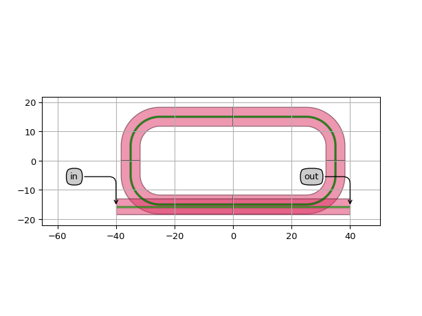
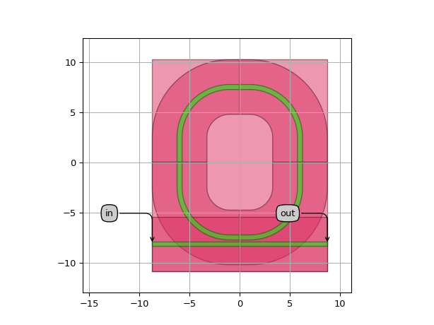
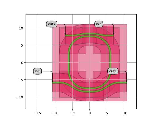
RingRect180DropFilter
- class picazzo3.filters.ring.cell.RingRect180DropFilter
Rectangular ring filter with two straight access waveguide. This component is often called a channel drop filter. The access waveguides are placed north and south of the Ring
The ring shape is a rounded rectangle of which the bend radius can be specified, as well as the horizontal and vertical straight sections. it is also possible to specify the rounding algorithm of the bends.
The waveguide template of the ring and the couplers can be chosen independently.
- Parameters:
- coupler_trace_templates: List with type restriction, allowed types: <class ‘ipkiss3.pcell.cell.pcell.PCell’>
list of trace_templates for the ring couplers. By default the same template as the ring is taken
- ring_trace_template: PCell and _WaveguideTemplate
Trace template for the ring waveguide
- ring_segments: List with type restriction, allowed types: <class ‘ipkiss3.pcell.cell.pcell.PCell’>
list of Ring PCells
- couplers: List with type restriction, allowed types: <class ‘ipkiss3.pcell.cell.pcell.PCell’>
list of coupler PCells
- name: String that contains only ISO/IEC 8859-1 (extended ASCII py3) or pure ASCII (py2) characters
The unique name of the pcell
- Other Parameters:
- ring_trace_templates: List with type restriction, allowed types: <class ‘ipkiss3.pcell.cell.pcell.PCell’>, locked
Trace templates for the ring segments. Locked, as there is only one segment in this Ring. Use ‘ring_trace_template’ instead.
Examples
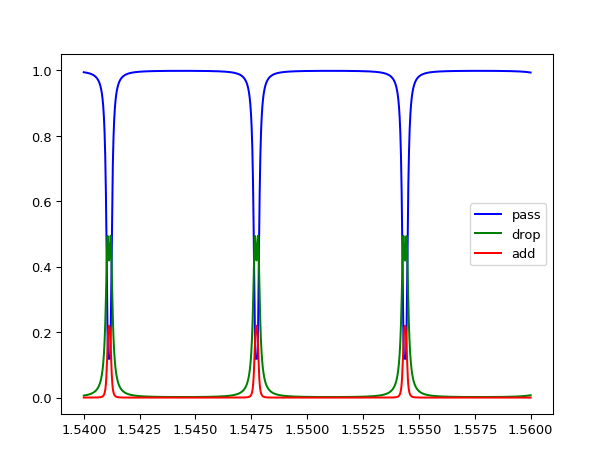
"""This example illustrates the basic ring resonator model without creating a layout.

It also illustrates the effect of resonance peak splitting due to back-reflection in the coupler.
"""
import si_fab.all as pdk  # noqa: F401
import pylab as plt
import numpy as np

from picazzo3.filters.ring import RingRect180DropFilter

# To get an FSR of 10 nm at 1.55 um, we use the following formula
n_g = 2.86  # default value used in picazzo3, see TECH.PCELLS.WG.DEFAULT
L_fsr_10nm = 1.55**2 / (n_g * 0.01)

# 1. Define the ring
my_ring = RingRect180DropFilter(name="my_example_ring")

# coupler parameters
cp = {
    "cross_coupling1": 1j * 0.0784**0.5,
    "straight_coupling1": 0.9216**0.5,
    "reflection_in1": 1j * 0.030,
}

my_ring_cm = my_ring.CircuitModel(
    ring_length=L_fsr_10nm,  # we can manually specify the ring length
    coupler_parameters=[cp, cp],  # 2 couplers
)

# 2. Simulate
wavelengths = np.linspace(1.54, 1.56, 2000)
R = my_ring_cm.get_smatrix(wavelengths=wavelengths)

# 3. Plot the results
plt.plot(wavelengths, np.abs(R["in1", "out1"]) ** 2, "b", label="pass")
plt.plot(wavelengths, np.abs(R["in1", "out2"]) ** 2, "g", label="drop")
plt.plot(wavelengths, np.abs(R["in1", "in2"]) ** 2, "r", label="add")
plt.legend()
plt.show()

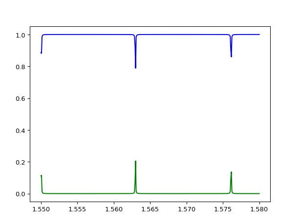
"""This example illustrates a simulation of a single ring resonator model based on the
layout that is first generated."""
import si_fab.all as pdk  # noqa: F401
import pylab as plt
import numpy as np

from picazzo3.filters.ring import RingRect180DropFilter

# 1. Define the ring
my_ring = RingRect180DropFilter(name="my_example_ring2")
my_ring.Layout(straights=(6.0, 0.0))

# set model in couplers and ring waveguides TODO: change the models
cp = {"delta_n_eff": 0.02}  # coupler parameters
for coupler in my_ring.couplers:
    coupler.set_default_view(coupler.SimpleCircuitModel)  # based on delta_n_eff
for ring_wg in my_ring.ring_segments:
    ring_wg.set_default_view(ring_wg.CircuitModel)  # based on the actual waveguide length

# ring model
my_ring_cm = my_ring.CircuitModel(coupler_parameters=[cp, cp])  # 2 couplers

# 2. Simulate
wavelengths = np.linspace(1.55, 1.58, 400)
R = my_ring_cm.get_smatrix(wavelengths=wavelengths)

# 3. Plot the results
plt.plot(wavelengths, np.abs(R["in1", "out1"]) ** 2, "b", label="pass")
plt.plot(wavelengths, np.abs(R["in1", "out2"]) ** 2, "g", label="drop")
plt.show()

Views
- class Layout
- Parameters:
- coupler_extensions: list<Coord2 and number >= 0>
additional length of the couplers. By default, the couplers will be extended to the size of the ring.
- coupler_lengths: list<number >= 0>
straight lengths of the coupling section. By default, same lengths as the ring will be used
- coupler_offsets: list<Real, number>
list of offsets of the ring couplers along the centerline
- coupler_spacings: list<Real, number>
list of centerline-to-centerline spacings of the ring couplers.When negative, the ring and coupler waveguide will cross, which ispossible when the ring traces template and the coupler trace templateare on different process layers (vertical couplers)
- straights: Coord2 and number >= 0
- shape_position: Coord2
Translation of the shape.
- coupler_transformations:
list of coupler transformations
- area_layer_on: ( bool, bool_ or int )
When True, the Ring area will be covered by i3.Rectangles on all cover layers of the ring waveguide template.
- coupler_parameters:
Parameters for the couplers. This is a list of dicts, and the length of the list should be the same as the number of couplers
- view_name: String that contains only alphanumeric characters from the ASCII set or contains _$. ASCII set is extended on PY3.
The name of the view
- manhattan: ( bool, bool_ or int )
Adds rectangular blocks in the bends to avoid as much as possible non-manhattan angles.
- angle_step: float and number > 0
Angle step for rounding.
- rounding_algorithm:
Rounding algorithm used to generate the bends. Can be circular, spline, ….
- bend_radius: float and number > 0
Bend radius for the auto-generated bends.
- Other Parameters:
- shape: locked
- shapes: locked
Shapes of the ring segments. Locked, as there is only 1 ring segment. Use ‘shape’ instead
Examples
import si_fab.all as pdk  # noqa: F401
from ipkiss3 import all as i3
from picazzo3.filters.ring import RingRect180DropFilter
from picazzo3.traces.wire_wg.trace import WireWaveguideTemplate

wg1_t = WireWaveguideTemplate(name="wg_template_6")
wg1_t.Layout(core_width=0.5)

wg2_t = WireWaveguideTemplate(name="wg_template_7")
wg2_t.Layout(core_width=0.4)

wg3_t = WireWaveguideTemplate(name="wg_template_8")
wg3_t.Layout(core_width=0.6)

ring = RingRect180DropFilter(
    name="my_ringrectdropring", ring_trace_template=wg1_t, coupler_trace_templates=[wg2_t, wg3_t]
)  # In a list!!!
layout = ring.Layout(
    coupler_spacings=[0.65, 0.70],  # This results in a 200nm and 250nm gap
    straights=(i3.TECH.WG.SHORT_STRAIGHT, i3.TECH.WG.SHORT_STRAIGHT + 3.0),
)

layout.visualize(annotate=True)
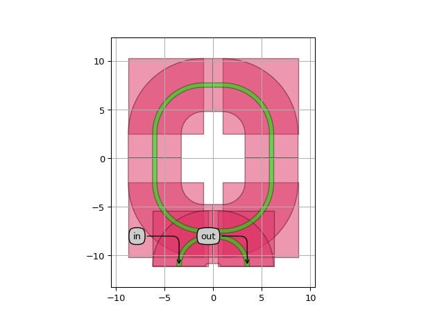
RingRoundedShape
- class picazzo3.filters.ring.cell.RingRoundedShape
A ring resonator based on a rounded shape, without couplers.
The Layout takes a shape, and a trace template. The trace template is turned into a RoundedTraceTemplate with the user supplied bend_radius and rounding_algorithm.
By default, this ring has no couplers. you can supply the couplers manually as a list of child cells through the property ‘couplers’, or you can subclass this PCell to define the couplers internally.
- Parameters:
- ring_trace_template: PCell and _WaveguideTemplate
Trace template for the ring waveguide
- ring_segments: List with type restriction, allowed types: <class ‘ipkiss3.pcell.cell.pcell.PCell’>
list of Ring PCells
- couplers: List with type restriction, allowed types: <class ‘ipkiss3.pcell.cell.pcell.PCell’>
list of coupler PCells
- name: String that contains only ISO/IEC 8859-1 (extended ASCII py3) or pure ASCII (py2) characters
The unique name of the pcell
- Other Parameters:
- ring_trace_templates: List with type restriction, allowed types: <class ‘ipkiss3.pcell.cell.pcell.PCell’>, locked
Trace templates for the ring segments. Locked, as there is only one segment in this Ring. Use ‘ring_trace_template’ instead.
See also
Views
- class Layout
- Parameters:
- shape_position: Coord2
Translation of the shape.
- shape: Shape
Shape of the ring
- coupler_transformations:
list of coupler transformations
- area_layer_on: ( bool, bool_ or int )
When True, the Ring area will be covered by i3.Rectangles on all cover layers of the ring waveguide template.
- coupler_parameters:
Parameters for the couplers. This is a list of dicts, and the length of the list should be the same as the number of couplers
- view_name: String that contains only alphanumeric characters from the ASCII set or contains _$. ASCII set is extended on PY3.
The name of the view
- manhattan: ( bool, bool_ or int )
Adds rectangular blocks in the bends to avoid as much as possible non-manhattan angles.
- angle_step: float and number > 0
Angle step for rounding.
- rounding_algorithm:
Rounding algorithm used to generate the bends. Can be circular, spline, ….
- bend_radius: float and number > 0
Bend radius for the auto-generated bends.
- Other Parameters:
- shapes: locked
Shapes of the ring segments. Locked, as there is only 1 ring segment. Use ‘shape’ instead
Examples
"""This example demonstrates a generic ring consisting of a user-defined control shape
which is drawn by rounding using the provided trace template with a given bend radius
"""
import si_fab.all as pdk  # noqa: F401
from ipkiss3 import all as i3
from picazzo3.filters.ring import RingRoundedShape
from picazzo3.traces.wire_wg.trace import WireWaveguideTemplate

wg_t = WireWaveguideTemplate(name="wg_template_2")
wg_t.Layout(core_width=0.45)

shape = i3.ShapeCross(box_size=26.0, thickness=13.0)

ring = RingRoundedShape(name="my_roundedring", ring_trace_template=wg_t)
layout = ring.Layout(shape=shape, bend_radius=3.0)

layout.visualize(annotate=True)
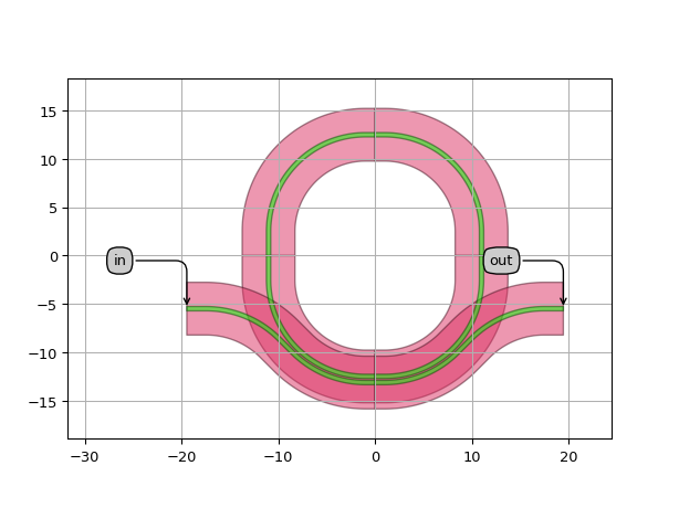
RingRectNotchFilter
- class picazzo3.filters.ring.cell.RingRectNotchFilter
Rectangular Ring resonator with one straight bus waveguide, which is placed on the South side of the ring. This type of filter is often called a ‘notch filter’ or ‘all-pass’ filter.
The ring shape is a rounded rectangle of which the bend radius can be specified, as well as the horizontal and vertical straight sections. it is also possible to specify the rounding algorithm of the bends.
The waveguide template of the ring and the couplers can be chosen independently.
- Parameters:
- coupler_trace_templates: List with type restriction, allowed types: <class ‘ipkiss3.pcell.cell.pcell.PCell’>
list of trace_templates for the ring couplers. By default the same template as the ring is taken
- ring_trace_template: PCell and _WaveguideTemplate
Trace template for the ring waveguide
- ring_segments: List with type restriction, allowed types: <class ‘ipkiss3.pcell.cell.pcell.PCell’>
list of Ring PCells
- couplers: List with type restriction, allowed types: <class ‘ipkiss3.pcell.cell.pcell.PCell’>
list of coupler PCells
- name: String that contains only ISO/IEC 8859-1 (extended ASCII py3) or pure ASCII (py2) characters
The unique name of the pcell
- Other Parameters:
- ring_trace_templates: List with type restriction, allowed types: <class ‘ipkiss3.pcell.cell.pcell.PCell’>, locked
Trace templates for the ring segments. Locked, as there is only one segment in this Ring. Use ‘ring_trace_template’ instead.
See also
Views
- class Layout
- Parameters:
- coupler_extensions: list<Coord2 and number >= 0>
additional length of the couplers. By default, the couplers will be extended to the size of the ring.
- coupler_lengths: list<number >= 0>
straight lengths of the coupling section. By default, same lengths as the ring will be used
- coupler_offsets: list<Real, number>
list of offsets of the ring couplers along the centerline
- coupler_spacings: list<Real, number>
list of centerline-to-centerline spacings of the ring couplers.When negative, the ring and coupler waveguide will cross, which ispossible when the ring traces template and the coupler trace templateare on different process layers (vertical couplers)
- straights: Coord2 and number >= 0
- shape_position: Coord2
Translation of the shape.
- coupler_transformations:
list of coupler transformations
- area_layer_on: ( bool, bool_ or int )
When True, the Ring area will be covered by i3.Rectangles on all cover layers of the ring waveguide template.
- coupler_parameters:
Parameters for the couplers. This is a list of dicts, and the length of the list should be the same as the number of couplers
- view_name: String that contains only alphanumeric characters from the ASCII set or contains _$. ASCII set is extended on PY3.
The name of the view
- manhattan: ( bool, bool_ or int )
Adds rectangular blocks in the bends to avoid as much as possible non-manhattan angles.
- angle_step: float and number > 0
Angle step for rounding.
- rounding_algorithm:
Rounding algorithm used to generate the bends. Can be circular, spline, ….
- bend_radius: float and number > 0
Bend radius for the auto-generated bends.
- Other Parameters:
- shape: locked
- shapes: locked
Shapes of the ring segments. Locked, as there is only 1 ring segment. Use ‘shape’ instead
Examples
import si_fab.all as pdk  # noqa: F401
from picazzo3.filters.ring import RingRectNotchFilter
from ipkiss3 import all as i3
from picazzo3.traces.wire_wg.trace import WireWaveguideTemplate

wg1_t = WireWaveguideTemplate(name="wg_template_4")
wg1_t.Layout(core_width=0.5)

wg2_t = WireWaveguideTemplate(name="wg_template_5")
wg2_t.Layout(core_width=0.4)

ring = RingRectNotchFilter(
    name="my_rectnotchring", ring_trace_template=wg1_t, coupler_trace_templates=[wg2_t]
)  # In a list!!!
layout = ring.Layout(
    coupler_spacings=[0.65],  # This results in a 200nm gap
    area_layer_on=True,
    straights=(i3.TECH.WG.SHORT_STRAIGHT, i3.TECH.WG.SHORT_STRAIGHT + 3.0),
)

layout.visualize(annotate=True)
RingRect180DropFilter
- class picazzo3.filters.ring.cell.RingRect180DropFilter
Rectangular ring filter with two straight access waveguide. This component is often called a channel drop filter. The access waveguides are placed north and south of the Ring
The ring shape is a rounded rectangle of which the bend radius can be specified, as well as the horizontal and vertical straight sections. it is also possible to specify the rounding algorithm of the bends.
The waveguide template of the ring and the couplers can be chosen independently.
- Parameters:
- coupler_trace_templates: List with type restriction, allowed types: <class ‘ipkiss3.pcell.cell.pcell.PCell’>
list of trace_templates for the ring couplers. By default the same template as the ring is taken
- ring_trace_template: PCell and _WaveguideTemplate
Trace template for the ring waveguide
- ring_segments: List with type restriction, allowed types: <class ‘ipkiss3.pcell.cell.pcell.PCell’>
list of Ring PCells
- couplers: List with type restriction, allowed types: <class ‘ipkiss3.pcell.cell.pcell.PCell’>
list of coupler PCells
- name: String that contains only ISO/IEC 8859-1 (extended ASCII py3) or pure ASCII (py2) characters
The unique name of the pcell
- Other Parameters:
- ring_trace_templates: List with type restriction, allowed types: <class ‘ipkiss3.pcell.cell.pcell.PCell’>, locked
Trace templates for the ring segments. Locked, as there is only one segment in this Ring. Use ‘ring_trace_template’ instead.
Examples
"""This example illustrates the basic ring resonator model without creating a layout.

It also illustrates the effect of resonance peak splitting due to back-reflection in the coupler.
"""
import si_fab.all as pdk  # noqa: F401
import pylab as plt
import numpy as np

from picazzo3.filters.ring import RingRect180DropFilter

# To get an FSR of 10 nm at 1.55 um, we use the following formula
n_g = 2.86  # default value used in picazzo3, see TECH.PCELLS.WG.DEFAULT
L_fsr_10nm = 1.55**2 / (n_g * 0.01)

# 1. Define the ring
my_ring = RingRect180DropFilter(name="my_example_ring")

# coupler parameters
cp = {
    "cross_coupling1": 1j * 0.0784**0.5,
    "straight_coupling1": 0.9216**0.5,
    "reflection_in1": 1j * 0.030,
}

my_ring_cm = my_ring.CircuitModel(
    ring_length=L_fsr_10nm,  # we can manually specify the ring length
    coupler_parameters=[cp, cp],  # 2 couplers
)

# 2. Simulate
wavelengths = np.linspace(1.54, 1.56, 2000)
R = my_ring_cm.get_smatrix(wavelengths=wavelengths)

# 3. Plot the results
plt.plot(wavelengths, np.abs(R["in1", "out1"]) ** 2, "b", label="pass")
plt.plot(wavelengths, np.abs(R["in1", "out2"]) ** 2, "g", label="drop")
plt.plot(wavelengths, np.abs(R["in1", "in2"]) ** 2, "r", label="add")
plt.legend()
plt.show()
"""This example illustrates a simulation of a single ring resonator model based on the
layout that is first generated."""
import si_fab.all as pdk  # noqa: F401
import pylab as plt
import numpy as np

from picazzo3.filters.ring import RingRect180DropFilter

# 1. Define the ring
my_ring = RingRect180DropFilter(name="my_example_ring2")
my_ring.Layout(straights=(6.0, 0.0))

# set model in couplers and ring waveguides TODO: change the models
cp = {"delta_n_eff": 0.02}  # coupler parameters
for coupler in my_ring.couplers:
    coupler.set_default_view(coupler.SimpleCircuitModel)  # based on delta_n_eff
for ring_wg in my_ring.ring_segments:
    ring_wg.set_default_view(ring_wg.CircuitModel)  # based on the actual waveguide length

# ring model
my_ring_cm = my_ring.CircuitModel(coupler_parameters=[cp, cp])  # 2 couplers

# 2. Simulate
wavelengths = np.linspace(1.55, 1.58, 400)
R = my_ring_cm.get_smatrix(wavelengths=wavelengths)

# 3. Plot the results
plt.plot(wavelengths, np.abs(R["in1", "out1"]) ** 2, "b", label="pass")
plt.plot(wavelengths, np.abs(R["in1", "out2"]) ** 2, "g", label="drop")
plt.show()
Views
- class Layout
- Parameters:
- coupler_extensions: list<Coord2 and number >= 0>
additional length of the couplers. By default, the couplers will be extended to the size of the ring.
- coupler_lengths: list<number >= 0>
straight lengths of the coupling section. By default, same lengths as the ring will be used
- coupler_offsets: list<Real, number>
list of offsets of the ring couplers along the centerline
- coupler_spacings: list<Real, number>
list of centerline-to-centerline spacings of the ring couplers.When negative, the ring and coupler waveguide will cross, which ispossible when the ring traces template and the coupler trace templateare on different process layers (vertical couplers)
- straights: Coord2 and number >= 0
- shape_position: Coord2
Translation of the shape.
- coupler_transformations:
list of coupler transformations
- area_layer_on: ( bool, bool_ or int )
When True, the Ring area will be covered by i3.Rectangles on all cover layers of the ring waveguide template.
- coupler_parameters:
Parameters for the couplers. This is a list of dicts, and the length of the list should be the same as the number of couplers
- view_name: String that contains only alphanumeric characters from the ASCII set or contains _$. ASCII set is extended on PY3.
The name of the view
- manhattan: ( bool, bool_ or int )
Adds rectangular blocks in the bends to avoid as much as possible non-manhattan angles.
- angle_step: float and number > 0
Angle step for rounding.
- rounding_algorithm:
Rounding algorithm used to generate the bends. Can be circular, spline, ….
- bend_radius: float and number > 0
Bend radius for the auto-generated bends.
- Other Parameters:
- shape: locked
- shapes: locked
Shapes of the ring segments. Locked, as there is only 1 ring segment. Use ‘shape’ instead
Examples
import si_fab.all as pdk  # noqa: F401
from ipkiss3 import all as i3
from picazzo3.filters.ring import RingRect180DropFilter
from picazzo3.traces.wire_wg.trace import WireWaveguideTemplate

wg1_t = WireWaveguideTemplate(name="wg_template_6")
wg1_t.Layout(core_width=0.5)

wg2_t = WireWaveguideTemplate(name="wg_template_7")
wg2_t.Layout(core_width=0.4)

wg3_t = WireWaveguideTemplate(name="wg_template_8")
wg3_t.Layout(core_width=0.6)

ring = RingRect180DropFilter(
    name="my_ringrectdropring", ring_trace_template=wg1_t, coupler_trace_templates=[wg2_t, wg3_t]
)  # In a list!!!
layout = ring.Layout(
    coupler_spacings=[0.65, 0.70],  # This results in a 200nm and 250nm gap
    straights=(i3.TECH.WG.SHORT_STRAIGHT, i3.TECH.WG.SHORT_STRAIGHT + 3.0),
)

layout.visualize(annotate=True)

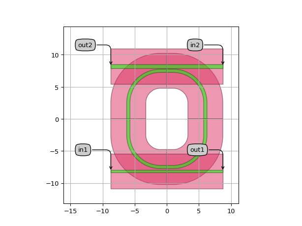
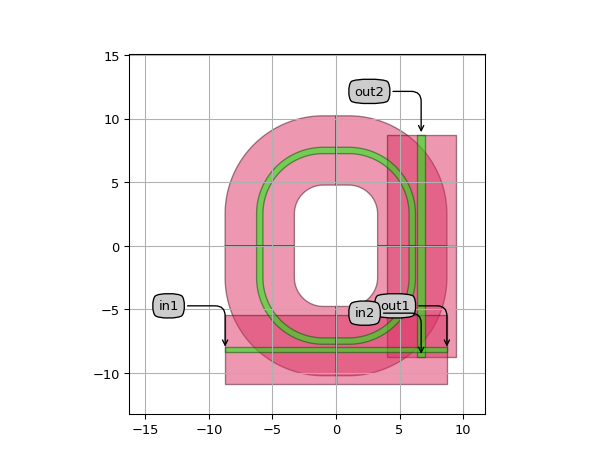
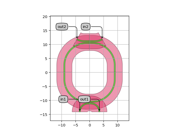
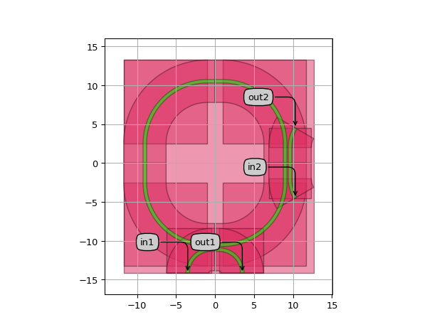
RingRect90DropFilter
- class picazzo3.filters.ring.cell.RingRect90DropFilter
Rectangular ring filter with two straight access waveguide. This component is often called a channel drop filter. The access waveguides are placed south and east of the Ring, at 90 degree angles.
The ring shape is a rounded rectangle of which the bend radius can be specified, as well as the horizontal and vertical straight sections. it is also possible to specify the rounding algorithm of the bends.
The waveguide template of the ring and the couplers can be chosen independently.
- Parameters:
- coupler_trace_templates: List with type restriction, allowed types: <class ‘ipkiss3.pcell.cell.pcell.PCell’>
list of trace_templates for the ring couplers. By default the same template as the ring is taken
- ring_trace_template: PCell and _WaveguideTemplate
Trace template for the ring waveguide
- ring_segments: List with type restriction, allowed types: <class ‘ipkiss3.pcell.cell.pcell.PCell’>
list of Ring PCells
- couplers: List with type restriction, allowed types: <class ‘ipkiss3.pcell.cell.pcell.PCell’>
list of coupler PCells
- name: String that contains only ISO/IEC 8859-1 (extended ASCII py3) or pure ASCII (py2) characters
The unique name of the pcell
- Other Parameters:
- ring_trace_templates: List with type restriction, allowed types: <class ‘ipkiss3.pcell.cell.pcell.PCell’>, locked
Trace templates for the ring segments. Locked, as there is only one segment in this Ring. Use ‘ring_trace_template’ instead.
Views
- class Layout
- Parameters:
- coupler_extensions: list<Coord2 and number >= 0>
additional length of the couplers. By default, the couplers will be extended to the size of the ring.
- coupler_lengths: list<number >= 0>
straight lengths of the coupling section. By default, same lengths as the ring will be used
- coupler_offsets: list<Real, number>
list of offsets of the ring couplers along the centerline
- coupler_spacings: list<Real, number>
list of centerline-to-centerline spacings of the ring couplers.When negative, the ring and coupler waveguide will cross, which ispossible when the ring traces template and the coupler trace templateare on different process layers (vertical couplers)
- straights: Coord2 and number >= 0
- shape_position: Coord2
Translation of the shape.
- coupler_transformations:
list of coupler transformations
- area_layer_on: ( bool, bool_ or int )
When True, the Ring area will be covered by i3.Rectangles on all cover layers of the ring waveguide template.
- coupler_parameters:
Parameters for the couplers. This is a list of dicts, and the length of the list should be the same as the number of couplers
- view_name: String that contains only alphanumeric characters from the ASCII set or contains _$. ASCII set is extended on PY3.
The name of the view
- manhattan: ( bool, bool_ or int )
Adds rectangular blocks in the bends to avoid as much as possible non-manhattan angles.
- angle_step: float and number > 0
Angle step for rounding.
- rounding_algorithm:
Rounding algorithm used to generate the bends. Can be circular, spline, ….
- bend_radius: float and number > 0
Bend radius for the auto-generated bends.
- Other Parameters:
- shape: locked
- shapes: locked
Shapes of the ring segments. Locked, as there is only 1 ring segment. Use ‘shape’ instead
Examples
import si_fab.all as pdk  # noqa: F401
from ipkiss3 import all as i3
from picazzo3.filters.ring import RingRect90DropFilter
from picazzo3.traces.wire_wg.trace import WireWaveguideTemplate

wg1_t = WireWaveguideTemplate(name="wg_template_9")
wg1_t.Layout(core_width=0.5)

wg2_t = WireWaveguideTemplate(name="wg_template_10")
wg2_t.Layout(core_width=0.4)

wg3_t = WireWaveguideTemplate(name="wg_template_11")
wg3_t.Layout(core_width=0.6)

ring = RingRect90DropFilter(
    name="my_rect90dropring", ring_trace_template=wg1_t, coupler_trace_templates=[wg2_t, wg3_t]
)  # In a list!!!
layout = ring.Layout(
    coupler_spacings=[0.65, 0.70],  # This results in a 200nm and 250nm gap
    straights=(i3.TECH.WG.SHORT_STRAIGHT, i3.TECH.WG.SHORT_STRAIGHT + 3.0),
)

layout.visualize(annotate=True)
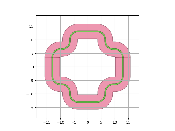
RingRectWrappedNotchFilter
- class picazzo3.filters.ring.cell.RingRectWrappedNotchFilter
Rectangular Ring resonator with one bus waveguide, which is placed on the South side of the ring. This type of filter is often called a ‘notch filter’ or ‘all-pass’ filter. The shape of the bus waveguide follows conformally the outline of the ring.
The ring shape is a rounded rectangle of which the bend radius can be specified, as well as the horizontal and vertical straight sections. it is also possible to specify the rounding algorithm of the bends.
The waveguide template of the ring and the couplers can be chosen independently.
- Parameters:
- coupler_trace_templates: List with type restriction, allowed types: <class ‘ipkiss3.pcell.cell.pcell.PCell’>
list of trace_templates for the ring couplers. By default the same template as the ring is taken
- ring_trace_template: PCell and _WaveguideTemplate
Trace template for the ring waveguide
- ring_segments: List with type restriction, allowed types: <class ‘ipkiss3.pcell.cell.pcell.PCell’>
list of Ring PCells
- couplers: List with type restriction, allowed types: <class ‘ipkiss3.pcell.cell.pcell.PCell’>
list of coupler PCells
- name: String that contains only ISO/IEC 8859-1 (extended ASCII py3) or pure ASCII (py2) characters
The unique name of the pcell
- Other Parameters:
- ring_trace_templates: List with type restriction, allowed types: <class ‘ipkiss3.pcell.cell.pcell.PCell’>, locked
Trace templates for the ring segments. Locked, as there is only one segment in this Ring. Use ‘ring_trace_template’ instead.
See also
Views
- class Layout
- Parameters:
- coupler_sbend_straights: list<number >= 0>
- coupler_angles: list<[-90,90]>
- coupler_rounding_algorithms:
rounding algorithm of the couplers. if None, same radius as the ring will be used
- coupler_radii: list<number >= 0>
radii of the couplers. if None, same radius as the ring will be used
- coupler_lengths: list<number >= 0>
straight lengths of the couplers. if None, same lengths as the ring will be used
- coupler_offsets: list<Real, number>
list of offsets of the ring couplers along the centerline
- coupler_spacings: list<Real, number>
list of centerline-to-centerline spacings of the ring couplers.When negative, the ring and coupler waveguide will cross, which ispossible when the ring traces template and the coupler trace templateare on different process layers (vertical couplers)
- straights: Coord2 and number >= 0
- shape_position: Coord2
Translation of the shape.
- coupler_transformations:
list of coupler transformations
- area_layer_on: ( bool, bool_ or int )
When True, the Ring area will be covered by i3.Rectangles on all cover layers of the ring waveguide template.
- coupler_parameters:
Parameters for the couplers. This is a list of dicts, and the length of the list should be the same as the number of couplers
- view_name: String that contains only alphanumeric characters from the ASCII set or contains _$. ASCII set is extended on PY3.
The name of the view
- manhattan: ( bool, bool_ or int )
Adds rectangular blocks in the bends to avoid as much as possible non-manhattan angles.
- angle_step: float and number > 0
Angle step for rounding.
- rounding_algorithm:
Rounding algorithm used to generate the bends. Can be circular, spline, ….
- bend_radius: float and number > 0
Bend radius for the auto-generated bends.
- Other Parameters:
- shape: locked
- shapes: locked
Shapes of the ring segments. Locked, as there is only 1 ring segment. Use ‘shape’ instead
Examples
import si_fab.all as pdk  # noqa: F401
from picazzo3.filters.ring import RingRectWrappedNotchFilter
import ipkiss3.all as i3

ring = RingRectWrappedNotchFilter(name="my_rectwrappednotchring")
layout = ring.Layout(
    bend_radius=10.0,
    straights=(i3.TECH.WG.SHORT_STRAIGHT, i3.TECH.WG.SHORT_STRAIGHT + 3.0),
    coupler_angles=[45.0, 45.0],
)

layout.visualize(annotate=True)
RingRectWrapped180DropFilter
- class picazzo3.filters.ring.cell.RingRectWrapped180DropFilter
Rectangular ring filter with two access waveguides. This component is often called a channel drop filter. The access waveguides are placed north and south of the Ring. The shape of the bus waveguide follows conformally the outline of the ring.
The ring shape is a rounded rectangle of which the bend radius can be specified, as well as the horizontal and vertical straight sections. it is also possible to specify the rounding algorithm of the bends.
The waveguide template of the ring and the couplers can be chosen independently.
- Parameters:
- coupler_trace_templates: List with type restriction, allowed types: <class ‘ipkiss3.pcell.cell.pcell.PCell’>
list of trace_templates for the ring couplers. By default the same template as the ring is taken
- ring_trace_template: PCell and _WaveguideTemplate
Trace template for the ring waveguide
- ring_segments: List with type restriction, allowed types: <class ‘ipkiss3.pcell.cell.pcell.PCell’>
list of Ring PCells
- couplers: List with type restriction, allowed types: <class ‘ipkiss3.pcell.cell.pcell.PCell’>
list of coupler PCells
- name: String that contains only ISO/IEC 8859-1 (extended ASCII py3) or pure ASCII (py2) characters
The unique name of the pcell
- Other Parameters:
- ring_trace_templates: List with type restriction, allowed types: <class ‘ipkiss3.pcell.cell.pcell.PCell’>, locked
Trace templates for the ring segments. Locked, as there is only one segment in this Ring. Use ‘ring_trace_template’ instead.
See also
Views
- class Layout
- Parameters:
- coupler_sbend_straights: list<number >= 0>
- coupler_angles: list<[-90,90]>
- coupler_rounding_algorithms:
rounding algorithm of the couplers. if None, same radius as the ring will be used
- coupler_radii: list<number >= 0>
radii of the couplers. if None, same radius as the ring will be used
- coupler_lengths: list<number >= 0>
straight lengths of the couplers. if None, same lengths as the ring will be used
- coupler_offsets: list<Real, number>
list of offsets of the ring couplers along the centerline
- coupler_spacings: list<Real, number>
list of centerline-to-centerline spacings of the ring couplers.When negative, the ring and coupler waveguide will cross, which ispossible when the ring traces template and the coupler trace templateare on different process layers (vertical couplers)
- straights: Coord2 and number >= 0
- shape_position: Coord2
Translation of the shape.
- coupler_transformations:
list of coupler transformations
- area_layer_on: ( bool, bool_ or int )
When True, the Ring area will be covered by i3.Rectangles on all cover layers of the ring waveguide template.
- coupler_parameters:
Parameters for the couplers. This is a list of dicts, and the length of the list should be the same as the number of couplers
- view_name: String that contains only alphanumeric characters from the ASCII set or contains _$. ASCII set is extended on PY3.
The name of the view
- manhattan: ( bool, bool_ or int )
Adds rectangular blocks in the bends to avoid as much as possible non-manhattan angles.
- angle_step: float and number > 0
Angle step for rounding.
- rounding_algorithm:
Rounding algorithm used to generate the bends. Can be circular, spline, ….
- bend_radius: float and number > 0
Bend radius for the auto-generated bends.
- Other Parameters:
- shape: locked
- shapes: locked
Shapes of the ring segments. Locked, as there is only 1 ring segment. Use ‘shape’ instead
Examples
import si_fab.all as pdk  # noqa: F401
from picazzo3.filters.ring import RingRectWrapped180DropFilter
import ipkiss3.all as i3

ring = RingRectWrapped180DropFilter(name="my_rectwrapped180dropring")
layout = ring.Layout(
    straights=(i3.TECH.WG.SHORT_STRAIGHT, i3.TECH.WG.SHORT_STRAIGHT + 3.0),
    coupler_angles=[30.0, 10.0],
    coupler_spacings=[1.0, 0.8],
    manhattan=True,
)

layout.visualize(annotate=True)
RingRectSymmNotchFilter
- class picazzo3.filters.ring.cell.RingRectSymmNotchFilter
Rectangular Ring resonator with one bus waveguide, which is placed on the South side of the ring. This type of filter is often called a ‘notch filter’ or ‘all-pass’ filter. The shape of the bus waveguide mirrors the shape of the ring, which makes the coupling section symmetric.
The ring shape is a rounded rectangle of which the bend radius can be specified, as well as the horizontal and vertical straight sections. it is also possible to specify the rounding algorithm of the bends.
The waveguide template of the ring and the couplers can be chosen independently.
- Parameters:
- coupler_trace_templates: List with type restriction, allowed types: <class ‘ipkiss3.pcell.cell.pcell.PCell’>
list of trace_templates for the ring couplers. By default the same template as the ring is taken
- ring_trace_template: PCell and _WaveguideTemplate
Trace template for the ring waveguide
- ring_segments: List with type restriction, allowed types: <class ‘ipkiss3.pcell.cell.pcell.PCell’>
list of Ring PCells
- couplers: List with type restriction, allowed types: <class ‘ipkiss3.pcell.cell.pcell.PCell’>
list of coupler PCells
- name: String that contains only ISO/IEC 8859-1 (extended ASCII py3) or pure ASCII (py2) characters
The unique name of the pcell
- Other Parameters:
- ring_trace_templates: List with type restriction, allowed types: <class ‘ipkiss3.pcell.cell.pcell.PCell’>, locked
Trace templates for the ring segments. Locked, as there is only one segment in this Ring. Use ‘ring_trace_template’ instead.
See also
Views
- class Layout
- Parameters:
- coupler_straights: list<number >= 0>
lengths of the straigth sections at the start and end of the couplers
- coupler_angles: list<[0,90]>
- coupler_rounding_algorithms:
rounding algorithm of the couplers. if None, same radius as the ring will be used
- coupler_radii: list<number >= 0>
radii of the couplers. if None, same radius as the ring will be used
- coupler_lengths: list<number >= 0>
straight lengths of the couplers. if None, same lengths as the ring will be used
- coupler_offsets: list<Real, number>
list of offsets of the ring couplers along the centerline
- coupler_spacings: list<Real, number>
list of centerline-to-centerline spacings of the ring couplers.When negative, the ring and coupler waveguide will cross, which ispossible when the ring traces template and the coupler trace templateare on different process layers (vertical couplers)
- straights: Coord2 and number >= 0
- shape_position: Coord2
Translation of the shape.
- coupler_transformations:
list of coupler transformations
- area_layer_on: ( bool, bool_ or int )
When True, the Ring area will be covered by i3.Rectangles on all cover layers of the ring waveguide template.
- coupler_parameters:
Parameters for the couplers. This is a list of dicts, and the length of the list should be the same as the number of couplers
- view_name: String that contains only alphanumeric characters from the ASCII set or contains _$. ASCII set is extended on PY3.
The name of the view
- manhattan: ( bool, bool_ or int )
Adds rectangular blocks in the bends to avoid as much as possible non-manhattan angles.
- angle_step: float and number > 0
Angle step for rounding.
- rounding_algorithm:
Rounding algorithm used to generate the bends. Can be circular, spline, ….
- bend_radius: float and number > 0
Bend radius for the auto-generated bends.
- Other Parameters:
- shape: locked
- shapes: locked
Shapes of the ring segments. Locked, as there is only 1 ring segment. Use ‘shape’ instead
Examples
import si_fab.all as pdk  # noqa: F401
from ipkiss3 import all as i3
from picazzo3.filters.ring import RingRectSymmNotchFilter

ring = RingRectSymmNotchFilter(name="my_rectsymmnotchring")
layout = ring.Layout(
    coupler_lengths=[1.0],
    coupler_radii=[3.0],
    straights=(i3.TECH.WG.SHORT_STRAIGHT, i3.TECH.WG.SHORT_STRAIGHT + 3.0),
    area_layer_on=False,
    manhattan=True,
)

layout.visualize(annotate=True)
RingRectSymm180DropFilter
- class picazzo3.filters.ring.cell.RingRectSymm180DropFilter
Rectangular ring filter with two access waveguide. This component is often called a channel drop filter. The access waveguides are placed north and south of the Ring. The shape of the bus waveguides mirrors the shape of the ring, which makes the coupling section symmetric.
The ring shape is a rounded rectangle of which the bend radius can be specified, as well as the horizontal and vertical straight sections. it is also possible to specify the rounding algorithm of the bends.
The waveguide template of the ring and the couplers can be chosen independently.
- Parameters:
- coupler_trace_templates: List with type restriction, allowed types: <class ‘ipkiss3.pcell.cell.pcell.PCell’>
list of trace_templates for the ring couplers. By default the same template as the ring is taken
- ring_trace_template: PCell and _WaveguideTemplate
Trace template for the ring waveguide
- ring_segments: List with type restriction, allowed types: <class ‘ipkiss3.pcell.cell.pcell.PCell’>
list of Ring PCells
- couplers: List with type restriction, allowed types: <class ‘ipkiss3.pcell.cell.pcell.PCell’>
list of coupler PCells
- name: String that contains only ISO/IEC 8859-1 (extended ASCII py3) or pure ASCII (py2) characters
The unique name of the pcell
- Other Parameters:
- ring_trace_templates: List with type restriction, allowed types: <class ‘ipkiss3.pcell.cell.pcell.PCell’>, locked
Trace templates for the ring segments. Locked, as there is only one segment in this Ring. Use ‘ring_trace_template’ instead.
Views
- class Layout
- Parameters:
- coupler_straights: list<number >= 0>
lengths of the straigth sections at the start and end of the couplers
- coupler_angles: list<[0,90]>
- coupler_rounding_algorithms:
rounding algorithm of the couplers. if None, same radius as the ring will be used
- coupler_radii: list<number >= 0>
radii of the couplers. if None, same radius as the ring will be used
- coupler_lengths: list<number >= 0>
straight lengths of the couplers. if None, same lengths as the ring will be used
- coupler_offsets: list<Real, number>
list of offsets of the ring couplers along the centerline
- coupler_spacings: list<Real, number>
list of centerline-to-centerline spacings of the ring couplers.When negative, the ring and coupler waveguide will cross, which ispossible when the ring traces template and the coupler trace templateare on different process layers (vertical couplers)
- straights: Coord2 and number >= 0
- shape_position: Coord2
Translation of the shape.
- coupler_transformations:
list of coupler transformations
- area_layer_on: ( bool, bool_ or int )
When True, the Ring area will be covered by i3.Rectangles on all cover layers of the ring waveguide template.
- coupler_parameters:
Parameters for the couplers. This is a list of dicts, and the length of the list should be the same as the number of couplers
- view_name: String that contains only alphanumeric characters from the ASCII set or contains _$. ASCII set is extended on PY3.
The name of the view
- manhattan: ( bool, bool_ or int )
Adds rectangular blocks in the bends to avoid as much as possible non-manhattan angles.
- angle_step: float and number > 0
Angle step for rounding.
- rounding_algorithm:
Rounding algorithm used to generate the bends. Can be circular, spline, ….
- bend_radius: float and number > 0
Bend radius for the auto-generated bends.
- Other Parameters:
- shape: locked
- shapes: locked
Shapes of the ring segments. Locked, as there is only 1 ring segment. Use ‘shape’ instead
Examples
import si_fab.all as pdk  # noqa: F401
from ipkiss3 import all as i3
from picazzo3.filters.ring import RingRectSymm180DropFilter

ring = RingRectSymm180DropFilter(name="my_rectsymm180dropring")
layout = ring.Layout(
    bend_radius=8.0,
    coupler_lengths=[1.0, 4.0],
    coupler_radii=[3.0, 5.0],
    coupler_angles=[90.0, 30.0],
    straights=(i3.TECH.WG.SHORT_STRAIGHT, i3.TECH.WG.SHORT_STRAIGHT + 3.0),
)

layout.visualize(annotate=True)
RingRectSymm90DropFilter
- class picazzo3.filters.ring.cell.RingRectSymm90DropFilter
Rectangular ring filter with two access waveguide. This component is often called a channel drop filter. The access waveguides are placed south and east of the Ring, at 90 degree angles. The shape of the bus waveguides mirrors the shape of the ring, which makes the coupling section symmetric.
The ring shape is a rounded rectangle of which the bend radius can be specified, as well as the horizontal and vertical straight sections. it is also possible to specify the rounding algorithm of the bends.
The waveguide template of the ring and the couplers can be chosen independently.
- Parameters:
- coupler_trace_templates: List with type restriction, allowed types: <class ‘ipkiss3.pcell.cell.pcell.PCell’>
list of trace_templates for the ring couplers. By default the same template as the ring is taken
- ring_trace_template: PCell and _WaveguideTemplate
Trace template for the ring waveguide
- ring_segments: List with type restriction, allowed types: <class ‘ipkiss3.pcell.cell.pcell.PCell’>
list of Ring PCells
- couplers: List with type restriction, allowed types: <class ‘ipkiss3.pcell.cell.pcell.PCell’>
list of coupler PCells
- name: String that contains only ISO/IEC 8859-1 (extended ASCII py3) or pure ASCII (py2) characters
The unique name of the pcell
- Other Parameters:
- ring_trace_templates: List with type restriction, allowed types: <class ‘ipkiss3.pcell.cell.pcell.PCell’>, locked
Trace templates for the ring segments. Locked, as there is only one segment in this Ring. Use ‘ring_trace_template’ instead.
Views
- class Layout
- Parameters:
- coupler_straights: list<number >= 0>
lengths of the straigth sections at the start and end of the couplers
- coupler_angles: list<[0,90]>
- coupler_rounding_algorithms:
rounding algorithm of the couplers. if None, same radius as the ring will be used
- coupler_radii: list<number >= 0>
radii of the couplers. if None, same radius as the ring will be used
- coupler_lengths: list<number >= 0>
straight lengths of the couplers. if None, same lengths as the ring will be used
- coupler_offsets: list<Real, number>
list of offsets of the ring couplers along the centerline
- coupler_spacings: list<Real, number>
list of centerline-to-centerline spacings of the ring couplers.When negative, the ring and coupler waveguide will cross, which ispossible when the ring traces template and the coupler trace templateare on different process layers (vertical couplers)
- straights: Coord2 and number >= 0
- shape_position: Coord2
Translation of the shape.
- coupler_transformations:
list of coupler transformations
- area_layer_on: ( bool, bool_ or int )
When True, the Ring area will be covered by i3.Rectangles on all cover layers of the ring waveguide template.
- coupler_parameters:
Parameters for the couplers. This is a list of dicts, and the length of the list should be the same as the number of couplers
- view_name: String that contains only alphanumeric characters from the ASCII set or contains _$. ASCII set is extended on PY3.
The name of the view
- manhattan: ( bool, bool_ or int )
Adds rectangular blocks in the bends to avoid as much as possible non-manhattan angles.
- angle_step: float and number > 0
Angle step for rounding.
- rounding_algorithm:
Rounding algorithm used to generate the bends. Can be circular, spline, ….
- bend_radius: float and number > 0
Bend radius for the auto-generated bends.
- Other Parameters:
- shape: locked
- shapes: locked
Shapes of the ring segments. Locked, as there is only 1 ring segment. Use ‘shape’ instead
Examples
import si_fab.all as pdk  # noqa: F401
from ipkiss3 import all as i3
from picazzo3.filters.ring import RingRectSymm90DropFilter

ring = RingRectSymm90DropFilter(name="my_rectsymm90dropring")
layout = ring.Layout(
    bend_radius=8.0,
    coupler_lengths=[1.0, 4.0],
    coupler_radii=[3.0, 5.0],
    coupler_angles=[90.0, 30.0],
    manhattan=True,
    straights=(i3.TECH.WG.SHORT_STRAIGHT, i3.TECH.WG.SHORT_STRAIGHT + 3.0),
)

layout.visualize(annotate=True)
RingRectSBendNotchFilter
- class picazzo3.filters.ring.cell.RingRectSBendNotchFilter
Rectangular Ring resonator with one bus waveguide, which is placed on the South side of the ring. The shape of the bus waveguide bends away from the ring, and then again horizontally, with an S-bend.
The ring shape is a rounded rectangle of which the bend radius can be specified, as well as the horizontal and vertical straight sections. it is also possible to specify the rounding algorithm of the bends.
The waveguide template of the ring and the couplers can be chosen independently.
- Parameters:
- coupler_trace_templates: List with type restriction, allowed types: <class ‘ipkiss3.pcell.cell.pcell.PCell’>
list of trace_templates for the ring couplers. By default the same template as the ring is taken
- ring_trace_template: PCell and _WaveguideTemplate
Trace template for the ring waveguide
- ring_segments: List with type restriction, allowed types: <class ‘ipkiss3.pcell.cell.pcell.PCell’>
list of Ring PCells
- couplers: List with type restriction, allowed types: <class ‘ipkiss3.pcell.cell.pcell.PCell’>
list of coupler PCells
- name: String that contains only ISO/IEC 8859-1 (extended ASCII py3) or pure ASCII (py2) characters
The unique name of the pcell
- Other Parameters:
- ring_trace_templates: List with type restriction, allowed types: <class ‘ipkiss3.pcell.cell.pcell.PCell’>, locked
Trace templates for the ring segments. Locked, as there is only one segment in this Ring. Use ‘ring_trace_template’ instead.
See also
Views
- class Layout
- Parameters:
- coupler_sbend_straights: list<number >= 0>
- coupler_angles: list<[0,90]>
- coupler_rounding_algorithms:
rounding algorithm of the couplers. if None, same radius as the ring will be used
- coupler_radii: list<number >= 0>
radii of the couplers. if None, same radius as the ring will be used
- coupler_lengths: list<number >= 0>
straight lengths of the couplers. if None, same lengths as the ring will be used
- coupler_offsets: list<Real, number>
list of offsets of the ring couplers along the centerline
- coupler_spacings: list<Real, number>
list of centerline-to-centerline spacings of the ring couplers.When negative, the ring and coupler waveguide will cross, which ispossible when the ring traces template and the coupler trace templateare on different process layers (vertical couplers)
- straights: Coord2 and number >= 0
- shape_position: Coord2
Translation of the shape.
- coupler_transformations:
list of coupler transformations
- area_layer_on: ( bool, bool_ or int )
When True, the Ring area will be covered by i3.Rectangles on all cover layers of the ring waveguide template.
- coupler_parameters:
Parameters for the couplers. This is a list of dicts, and the length of the list should be the same as the number of couplers
- view_name: String that contains only alphanumeric characters from the ASCII set or contains _$. ASCII set is extended on PY3.
The name of the view
- manhattan: ( bool, bool_ or int )
Adds rectangular blocks in the bends to avoid as much as possible non-manhattan angles.
- angle_step: float and number > 0
Angle step for rounding.
- rounding_algorithm:
Rounding algorithm used to generate the bends. Can be circular, spline, ….
- bend_radius: float and number > 0
Bend radius for the auto-generated bends.
- Other Parameters:
- shape: locked
- shapes: locked
Shapes of the ring segments. Locked, as there is only 1 ring segment. Use ‘shape’ instead
Examples
import si_fab.all as pdk  # noqa: F401
from picazzo3.filters.ring import RingRectSBendNotchFilter
import ipkiss3.all as i3

ring = RingRectSBendNotchFilter(name="my_ring12")
layout = ring.Layout(
    straights=(i3.TECH.WG.SHORT_STRAIGHT, i3.TECH.WG.SHORT_STRAIGHT + 3.0),
    coupler_sbend_straights=[6.0],
    manhattan=True,
    area_layer_on=False,
)

layout.visualize(annotate=True)
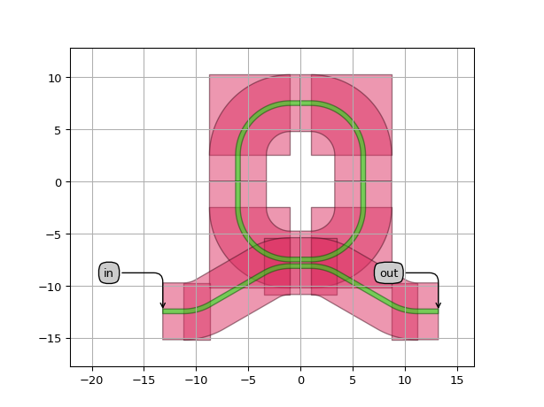
RingRectSBend180DropFilter
- class picazzo3.filters.ring.cell.RingRectSBend180DropFilter
Rectangular ring filter with two access waveguides. This component is often called a channel drop filter. The access waveguides are placed north and south of the Ring. The shapes of the bus waveguides bends away from the ring, and then again horizontally, with an S-bend.
The ring shape is a rounded rectangle of which the bend radius can be specified, as well as the horizontal and vertical straight sections. it is also possible to specify the rounding algorithm of the bends.
The waveguide template of the ring and the couplers can be chosen independently.
- Parameters:
- coupler_trace_templates: List with type restriction, allowed types: <class ‘ipkiss3.pcell.cell.pcell.PCell’>
list of trace_templates for the ring couplers. By default the same template as the ring is taken
- ring_trace_template: PCell and _WaveguideTemplate
Trace template for the ring waveguide
- ring_segments: List with type restriction, allowed types: <class ‘ipkiss3.pcell.cell.pcell.PCell’>
list of Ring PCells
- couplers: List with type restriction, allowed types: <class ‘ipkiss3.pcell.cell.pcell.PCell’>
list of coupler PCells
- name: String that contains only ISO/IEC 8859-1 (extended ASCII py3) or pure ASCII (py2) characters
The unique name of the pcell
- Other Parameters:
- ring_trace_templates: List with type restriction, allowed types: <class ‘ipkiss3.pcell.cell.pcell.PCell’>, locked
Trace templates for the ring segments. Locked, as there is only one segment in this Ring. Use ‘ring_trace_template’ instead.
See also
Views
- class Layout
- Parameters:
- coupler_sbend_straights: list<number >= 0>
- coupler_angles: list<[0,90]>
- coupler_rounding_algorithms:
rounding algorithm of the couplers. if None, same radius as the ring will be used
- coupler_radii: list<number >= 0>
radii of the couplers. if None, same radius as the ring will be used
- coupler_lengths: list<number >= 0>
straight lengths of the couplers. if None, same lengths as the ring will be used
- coupler_offsets: list<Real, number>
list of offsets of the ring couplers along the centerline
- coupler_spacings: list<Real, number>
list of centerline-to-centerline spacings of the ring couplers.When negative, the ring and coupler waveguide will cross, which ispossible when the ring traces template and the coupler trace templateare on different process layers (vertical couplers)
- straights: Coord2 and number >= 0
- shape_position: Coord2
Translation of the shape.
- coupler_transformations:
list of coupler transformations
- area_layer_on: ( bool, bool_ or int )
When True, the Ring area will be covered by i3.Rectangles on all cover layers of the ring waveguide template.
- coupler_parameters:
Parameters for the couplers. This is a list of dicts, and the length of the list should be the same as the number of couplers
- view_name: String that contains only alphanumeric characters from the ASCII set or contains _$. ASCII set is extended on PY3.
The name of the view
- manhattan: ( bool, bool_ or int )
Adds rectangular blocks in the bends to avoid as much as possible non-manhattan angles.
- angle_step: float and number > 0
Angle step for rounding.
- rounding_algorithm:
Rounding algorithm used to generate the bends. Can be circular, spline, ….
- bend_radius: float and number > 0
Bend radius for the auto-generated bends.
- Other Parameters:
- shape: locked
- shapes: locked
Shapes of the ring segments. Locked, as there is only 1 ring segment. Use ‘shape’ instead
Examples
import si_fab.all as pdk  # noqa: F401
from picazzo3.filters.ring import RingRectSBend180DropFilter
import ipkiss3.all as i3

ring = RingRectSBend180DropFilter(name="my_rectsbend180dropring")
layout = ring.Layout(
    straights=(i3.TECH.WG.SHORT_STRAIGHT, i3.TECH.WG.SHORT_STRAIGHT + 3.0),
    coupler_angles=[30.0, 10.0],
    coupler_spacings=[1.0, 0.8],
    coupler_lengths=[6.0, 2.0],
    coupler_radii=[3.0, 7.0],
    manhattan=True,
    area_layer_on=False,
)

layout.visualize(annotate=True)
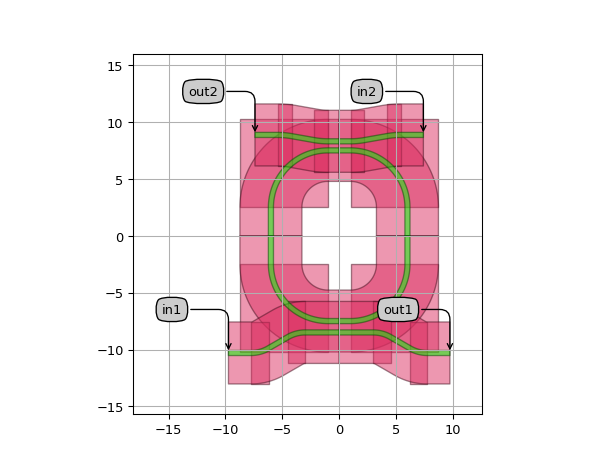
Multi-mode Interferometers
MMITapered
- class picazzo3.filters.mmi.MMITapered
Rectangular multimode interferometer, generated from a waveguide template with tapers.
- Parameters:
- output_trace_templates: List with type restriction, allowed types: <class ‘ipkiss3.pcell.cell.pcell.PCell’>
List of the output trace templates.
- input_trace_templates: List with type restriction, allowed types: <class ‘ipkiss3.pcell.cell.pcell.PCell’>
List of the input trace templates.
- mmi_trace_template: PCell and _WaveguideTemplate
Trace template used for the MMI section
- trace_template: ( PCell and _WaveguideTemplate ), *None allowed*
Template for all ports, defaults to TECH.PCELLS.WG.DEFAULT.When set to None, the waveguide templates of the ports will be used.
- transition_database: AutoTransitionDatabase
AutoTransitionDatabase in which the correct transition between the two trace templates can be looked up.
- transitions: List with type restriction, allowed types: <class ‘ipkiss3.pcell.cell.pcell.PCell’>
List of transitions that is used on this MMI. By default Autotracetransition is used on all the transitions
- port_labels: ( List with type restriction, allowed types: <class ‘str’> ), *None allowed*
Labels of the ports to be processed. Set to None to process all ports.
- external_port_names: str
Dictionary for remapping of the port names of the contents to the external ports
- name: String that contains only ISO/IEC 8859-1 (extended ASCII py3) or pure ASCII (py2) characters
The unique name of the pcell
- Other Parameters:
- mmi_trace: PCell, locked
Trace of the MMI section
- n_outputs: int and number > 0, locked
Number of output channels.
- n_inputs: int and number > 0, locked
Number of input channels.
- trace_templates: List with type restriction, allowed types: <class ‘ipkiss3.pcell.cell.pcell.PCell’>, locked
list of templates to apply to all ports
- contents: PCell, locked
Contains the base MMI without the tapers
Views
- class Layout
- Parameters:
- output_y_positions: list<Real, number>
Positions in the y direction at the output where ports are be added
- input_y_positions: list<Real, number>
Positions in the y direction at the input where ports are be added
- transition_length: ( float and Real, number and number >= 0 ), *None allowed*
Length of the transition. Set to None to take the standard transition length.
- zero_length_if_identical: ( bool, bool_ or int )
uses a zero-length transition if the trace templates are identical
- flatten_transitions: ( bool, bool_ or int )
if true, flattens the transitions one level
- straight_extension: ( Coord2 and number >= 0 ), *None allowed*
Tuple: straight extensions of the transitions. Set to None to take the standard straight extensions
- length: float and number > 0
Length of the MMI
- contents_transformation: GenericNoDistortTransform
transformation to apply to the contents
- flatten_contents: ( bool, bool_ or int )
if True, it will insert the contents as elements in the layout, rather than as an Instance
- view_name: String that contains only alphanumeric characters from the ASCII set or contains _$. ASCII set is extended on PY3.
The name of the view
- Other Parameters:
- transition_lengths: locked
Examples
import si_fab.all as pdk  # noqa: F401
from picazzo3.filters.mmi.cell import MMITapered
from picazzo3.traces.wire_wg.trace import WireWaveguideTemplate
import ipkiss3.all as i3

mmi_trace_template = WireWaveguideTemplate()
mmi_trace_template.Layout(core_width=6.0, cladding_width=10.0)

mmi_access_template = WireWaveguideTemplate()
mmi_access_template.Layout(core_width=1.0, cladding_width=5.0)

MMI = MMITapered(
    mmi_trace_template=mmi_trace_template,
    input_trace_templates=[mmi_access_template],
    output_trace_templates=[mmi_access_template],
    trace_template=i3.TECH.PCELLS.WG.DEFAULT,
)
layout = MMI.Layout(transition_length=5.0, length=10.0, input_y_positions=[0.0], output_y_positions=[0.0])
layout.visualize(annotate=True)
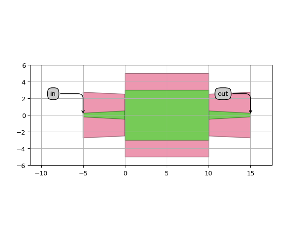
Tapered MMI with matched claddings:
import si_fab.all as pdk  # noqa: F401
from picazzo3.filters.mmi.cell import MMITapered
from picazzo3.traces.wire_wg.trace import WireWaveguideTemplate
import ipkiss3.all as i3
import numpy as np

# This example illustrates a tapered MMI where the access waveguides are calculated in
# such a way that the cladding of the mmi matches naturally transitions to the cladding
# of the access waveguides.

mmi_cladding_width = 15.0  # Cladding width of the MMI section.
mmi_access_core_width = 1.0  # Core width of the access waveguides.
input_y_positions = [0.0]  # Input position of the access waveguides
output_y_positions = [-1.5, 0, 1.5]  # Output positions of the access waveguides

# We create the trace template for the MMI section
mmi_trace_template = WireWaveguideTemplate()
mmi_trace_template.Layout(core_width=10.0, cladding_width=mmi_cladding_width)

# We create the template for the access waveguide at the input side.
mmi_access_template = WireWaveguideTemplate()
mmi_access_template.Layout(core_width=mmi_access_core_width, cladding_width=mmi_cladding_width)
output_trace_templates = []

# We create the templates for the access waveguides at the output side. We calculate the
# cladding width of the access waveguides so that the tapers would transition to the
# cladding of the MMI.

for cnt, pos in enumerate(output_y_positions):
    template = WireWaveguideTemplate()
    height_cladding = mmi_cladding_width
    width_to_top = height_cladding / 2 - pos
    width_to_bottom = pos + height_cladding / 2
    # Just as wide as to reach the nearest cladding of the mmi.
    access_cladding_width = np.min([width_to_top, width_to_bottom]) * 2
    template.Layout(core_width=mmi_access_core_width, cladding_width=access_cladding_width)
    output_trace_templates.append(template)

# We create the tapered MMI
MMI_with_matched_claddings = MMITapered(
    mmi_trace_template=mmi_trace_template,
    input_trace_templates=[mmi_access_template],
    output_trace_templates=output_trace_templates,
    trace_template=i3.TECH.PCELLS.WG.DEFAULT,
)

layout = MMI_with_matched_claddings.Layout(
    transition_length=5.0,
    length=10.0,
    input_y_positions=input_y_positions,
    output_y_positions=output_y_positions,
)
layout.visualize(annotate=True)
MMIIdenticalTapered
- class picazzo3.filters.mmi.MMIIdenticalTapered
Rectangular multimode interferometer, generated from a trace template with identical input and output trace_templates and with tapers.
- Parameters:
- output_trace_template: PCell
Output trace template.
- input_trace_template: PCell
Input trace template.
- mmi_trace_template: PCell and _WaveguideTemplate
Trace template used for the MMI section
- n_outputs: int and number > 0
Number of output channels.
- n_inputs: int and number > 0
Number of input channels
- trace_template: ( PCell and _WaveguideTemplate ), *None allowed*
Template for all ports, defaults to TECH.PCELLS.WG.DEFAULT.When set to None, the waveguide templates of the ports will be used.
- transition_database: AutoTransitionDatabase
AutoTransitionDatabase in which the correct transition between the two trace templates can be looked up.
- transitions: List with type restriction, allowed types: <class ‘ipkiss3.pcell.cell.pcell.PCell’>
List of transitions that is used on this MMI. By default Autotracetransition is used on all the transitions
- port_labels: ( List with type restriction, allowed types: <class ‘str’> ), *None allowed*
Labels of the ports to be processed. Set to None to process all ports.
- external_port_names: str
Dictionary for remapping of the port names of the contents to the external ports
- name: String that contains only ISO/IEC 8859-1 (extended ASCII py3) or pure ASCII (py2) characters
The unique name of the pcell
- Other Parameters:
- mmi_trace: PCell, locked
Trace of the MMI section
- output_trace_templates: List with type restriction, allowed types: <class ‘ipkiss3.pcell.cell.pcell.PCell’>, locked
List of the output trace templates.
- input_trace_templates: List with type restriction, allowed types: <class ‘ipkiss3.pcell.cell.pcell.PCell’>, locked
List of the input trace templates.
- trace_templates: List with type restriction, allowed types: <class ‘ipkiss3.pcell.cell.pcell.PCell’>, locked
list of templates to apply to all ports
- contents: PCell, locked
Contains the base MMI without the tapers
Views
- class Layout
- Parameters:
- output_y_positions: list<Real, number>
Positions in the y direction at the output where ports are be added
- input_y_positions: list<Real, number>
Positions in the y direction at the input where ports are be added
- transition_length: ( float and Real, number and number >= 0 ), *None allowed*
Length of the transition. Set to None to take the standard transition length.
- zero_length_if_identical: ( bool, bool_ or int )
uses a zero-length transition if the trace templates are identical
- flatten_transitions: ( bool, bool_ or int )
if true, flattens the transitions one level
- straight_extension: ( Coord2 and number >= 0 ), *None allowed*
Tuple: straight extensions of the transitions. Set to None to take the standard straight extensions
- length: float and number > 0
Length of the MMI
- contents_transformation: GenericNoDistortTransform
transformation to apply to the contents
- flatten_contents: ( bool, bool_ or int )
if True, it will insert the contents as elements in the layout, rather than as an Instance
- view_name: String that contains only alphanumeric characters from the ASCII set or contains _$. ASCII set is extended on PY3.
The name of the view
- Other Parameters:
- transition_lengths: locked
Examples
import si_fab.all as pdk  # noqa: F401
from picazzo3.filters.mmi.cell import MMIIdenticalTapered
from picazzo3.traces.wire_wg.trace import WireWaveguideTemplate
import ipkiss3.all as i3

mmi_trace_template = WireWaveguideTemplate()
mmi_trace_template.Layout(core_width=6.0, cladding_width=10.0)

mmi_access_template = WireWaveguideTemplate()
mmi_access_template.Layout(core_width=1.0, cladding_width=5.0)

MMI = MMIIdenticalTapered(
    mmi_trace_template=mmi_trace_template,
    input_trace_template=mmi_access_template,
    output_trace_template=mmi_access_template,
    trace_template=i3.TECH.PCELLS.WG.DEFAULT,
    n_inputs=3,
    n_outputs=2,
)
layout = MMI.Layout(
    transition_length=5.0, length=10.0, input_y_positions=[-2.0, 0.0, 2.0], output_y_positions=[-1.0, 1.0]
)
layout.visualize(annotate=True)
MMISymmetricTapered
- class picazzo3.filters.mmi.MMISymmetricTapered
MMI with symmetrically distributed access templates and with tapers. This is usually useful when the MMI is used a splitter or combiner.
- Parameters:
- output_trace_template: PCell
Output trace template.
- input_trace_template: PCell
Input trace template.
- mmi_trace_template: PCell and _WaveguideTemplate
Trace template used for the MMI section
- n_outputs: int and number > 0
Number of output channels.
- n_inputs: int and number > 0
Number of input channels
- trace_template: ( PCell and _WaveguideTemplate ), *None allowed*
Template for all ports, defaults to TECH.PCELLS.WG.DEFAULT.When set to None, the waveguide templates of the ports will be used.
- transition_database: AutoTransitionDatabase
AutoTransitionDatabase in which the correct transition between the two trace templates can be looked up.
- transitions: List with type restriction, allowed types: <class ‘ipkiss3.pcell.cell.pcell.PCell’>
List of transitions that is used on this MMI. By default Autotracetransition is used on all the transitions
- port_labels: ( List with type restriction, allowed types: <class ‘str’> ), *None allowed*
Labels of the ports to be processed. Set to None to process all ports.
- external_port_names: str
Dictionary for remapping of the port names of the contents to the external ports
- name: String that contains only ISO/IEC 8859-1 (extended ASCII py3) or pure ASCII (py2) characters
The unique name of the pcell
- Other Parameters:
- mmi_trace: PCell, locked
Trace of the MMI section
- output_trace_templates: List with type restriction, allowed types: <class ‘ipkiss3.pcell.cell.pcell.PCell’>, locked
List of the output trace templates.
- input_trace_templates: List with type restriction, allowed types: <class ‘ipkiss3.pcell.cell.pcell.PCell’>, locked
List of the input trace templates.
- trace_templates: List with type restriction, allowed types: <class ‘ipkiss3.pcell.cell.pcell.PCell’>, locked
list of templates to apply to all ports
- contents: PCell, locked
Contains the base MMI without the tapers
Views
- class Layout
- Parameters:
- trace_spacing: float and Real, number and number >= 0
Offset between the traces at the input and the output
- transition_length: ( float and Real, number and number >= 0 ), *None allowed*
Length of the transition. Set to None to take the standard transition length.
- zero_length_if_identical: ( bool, bool_ or int )
uses a zero-length transition if the trace templates are identical
- flatten_transitions: ( bool, bool_ or int )
if true, flattens the transitions one level
- straight_extension: ( Coord2 and number >= 0 ), *None allowed*
Tuple: straight extensions of the transitions. Set to None to take the standard straight extensions
- length: float and number > 0
Length of the MMI
- contents_transformation: GenericNoDistortTransform
transformation to apply to the contents
- flatten_contents: ( bool, bool_ or int )
if True, it will insert the contents as elements in the layout, rather than as an Instance
- view_name: String that contains only alphanumeric characters from the ASCII set or contains _$. ASCII set is extended on PY3.
The name of the view
- Other Parameters:
- output_y_positions: list<Real, number>, locked
Positions in the y direction at the output where access waveguides are be added
- input_y_positions: list<Real, number>, locked
Positions in the y direction at the input where ports are be added
- transition_lengths: locked
Examples
import si_fab.all as pdk  # noqa: F401
from picazzo3.filters.mmi.cell import MMISymmetricTapered
from picazzo3.traces.wire_wg.trace import WireWaveguideTemplate
import ipkiss3.all as i3

mmi_trace_template = WireWaveguideTemplate()
mmi_trace_template.Layout(core_width=6.0, cladding_width=10.0)

mmi_access_template = WireWaveguideTemplate()
mmi_access_template.Layout(core_width=1.0, cladding_width=5.0)

MMI = MMISymmetricTapered(
    mmi_trace_template=mmi_trace_template,
    input_trace_template=mmi_access_template,
    output_trace_template=mmi_access_template,
    trace_template=i3.TECH.PCELLS.WG.DEFAULT,
    n_inputs=3,
    n_outputs=2,
)
layout = MMI.Layout(transition_length=5.0, length=10.0, trace_spacing=2.0)
layout.visualize(annotate=True)

MMI1x2Tapered
- class picazzo3.filters.mmi.MMI1x2Tapered
MMI with one access waveguide and two output waveguides and with tapers that symmetrically distributed. This is usually useful when the MMI is used as a splitter.
- Parameters:
- output_trace_template: PCell
Output trace template.
- input_trace_template: PCell
Input trace template.
- mmi_trace_template: PCell and _WaveguideTemplate
Trace template used for the MMI section
- trace_template: ( PCell and _WaveguideTemplate ), *None allowed*
Template for all ports, defaults to TECH.PCELLS.WG.DEFAULT.When set to None, the waveguide templates of the ports will be used.
- transition_database: AutoTransitionDatabase
AutoTransitionDatabase in which the correct transition between the two trace templates can be looked up.
- transitions: List with type restriction, allowed types: <class ‘ipkiss3.pcell.cell.pcell.PCell’>
List of transitions that is used on this MMI. By default Autotracetransition is used on all the transitions
- port_labels: ( List with type restriction, allowed types: <class ‘str’> ), *None allowed*
Labels of the ports to be processed. Set to None to process all ports.
- external_port_names: str
Dictionary for remapping of the port names of the contents to the external ports
- name: String that contains only ISO/IEC 8859-1 (extended ASCII py3) or pure ASCII (py2) characters
The unique name of the pcell
- Other Parameters:
- mmi_trace: PCell, locked
Trace of the MMI section
- output_trace_templates: List with type restriction, allowed types: <class ‘ipkiss3.pcell.cell.pcell.PCell’>, locked
List of the output trace templates.
- input_trace_templates: List with type restriction, allowed types: <class ‘ipkiss3.pcell.cell.pcell.PCell’>, locked
List of the input trace templates.
- n_outputs: int and number > 0, locked
Number of output channels.
- n_inputs: int and number > 0, locked
Number of input channels.
- trace_templates: List with type restriction, allowed types: <class ‘ipkiss3.pcell.cell.pcell.PCell’>, locked
list of templates to apply to all ports
- contents: PCell, locked
Contains the base MMI without the tapers
Views
- class Layout
- Parameters:
- trace_spacing: float and Real, number and number >= 0
Offset between the traces at the input and the output
- transition_length: ( float and Real, number and number >= 0 ), *None allowed*
Length of the transition. Set to None to take the standard transition length.
- zero_length_if_identical: ( bool, bool_ or int )
uses a zero-length transition if the trace templates are identical
- flatten_transitions: ( bool, bool_ or int )
if true, flattens the transitions one level
- straight_extension: ( Coord2 and number >= 0 ), *None allowed*
Tuple: straight extensions of the transitions. Set to None to take the standard straight extensions
- length: float and number > 0
Length of the MMI
- contents_transformation: GenericNoDistortTransform
transformation to apply to the contents
- flatten_contents: ( bool, bool_ or int )
if True, it will insert the contents as elements in the layout, rather than as an Instance
- view_name: String that contains only alphanumeric characters from the ASCII set or contains _$. ASCII set is extended on PY3.
The name of the view
- Other Parameters:
- output_y_positions: list<Real, number>, locked
Positions in the y direction at the output where access waveguides are be added
- input_y_positions: list<Real, number>, locked
Positions in the y direction at the input where ports are be added
- transition_lengths: locked
Examples
import si_fab.all as pdk  # noqa: F401
from picazzo3.filters.mmi.cell import MMI1x2Tapered
from picazzo3.traces.wire_wg.trace import WireWaveguideTemplate
import ipkiss3.all as i3

mmi_trace_template = WireWaveguideTemplate()
mmi_trace_template.Layout(core_width=6.0, cladding_width=10.0)

mmi_access_template = WireWaveguideTemplate()
mmi_access_template.Layout(core_width=1.0, cladding_width=5.0)

MMI = MMI1x2Tapered(
    mmi_trace_template=mmi_trace_template,
    input_trace_template=mmi_access_template,
    output_trace_template=mmi_access_template,
    trace_template=i3.TECH.PCELLS.WG.DEFAULT,
)
layout = MMI.Layout(transition_length=5.0, length=10.0, trace_spacing=2.0)
layout.visualize(annotate=True)
MMI2x1Tapered
- class picazzo3.filters.mmi.MMI2x1Tapered
MMI with two access waveguides and one output waveguides and with tapers that symmetrically distributed. This is usually useful when the MMI is used as a combiner.
- Parameters:
- output_trace_template: PCell
Output trace template.
- input_trace_template: PCell
Input trace template.
- mmi_trace_template: PCell and _WaveguideTemplate
Trace template used for the MMI section
- trace_template: ( PCell and _WaveguideTemplate ), *None allowed*
Template for all ports, defaults to TECH.PCELLS.WG.DEFAULT.When set to None, the waveguide templates of the ports will be used.
- transition_database: AutoTransitionDatabase
AutoTransitionDatabase in which the correct transition between the two trace templates can be looked up.
- transitions: List with type restriction, allowed types: <class ‘ipkiss3.pcell.cell.pcell.PCell’>
List of transitions that is used on this MMI. By default Autotracetransition is used on all the transitions
- port_labels: ( List with type restriction, allowed types: <class ‘str’> ), *None allowed*
Labels of the ports to be processed. Set to None to process all ports.
- external_port_names: str
Dictionary for remapping of the port names of the contents to the external ports
- name: String that contains only ISO/IEC 8859-1 (extended ASCII py3) or pure ASCII (py2) characters
The unique name of the pcell
- Other Parameters:
- mmi_trace: PCell, locked
Trace of the MMI section
- output_trace_templates: List with type restriction, allowed types: <class ‘ipkiss3.pcell.cell.pcell.PCell’>, locked
List of the output trace templates.
- input_trace_templates: List with type restriction, allowed types: <class ‘ipkiss3.pcell.cell.pcell.PCell’>, locked
List of the input trace templates.
- n_outputs: int and number > 0, locked
Number of output channels.
- n_inputs: int and number > 0, locked
Number of input channels.
- trace_templates: List with type restriction, allowed types: <class ‘ipkiss3.pcell.cell.pcell.PCell’>, locked
list of templates to apply to all ports
- contents: PCell, locked
Contains the base MMI without the tapers
Views
- class Layout
- Parameters:
- trace_spacing: float and Real, number and number >= 0
Offset between the traces at the input and the output
- transition_length: ( float and Real, number and number >= 0 ), *None allowed*
Length of the transition. Set to None to take the standard transition length.
- zero_length_if_identical: ( bool, bool_ or int )
uses a zero-length transition if the trace templates are identical
- flatten_transitions: ( bool, bool_ or int )
if true, flattens the transitions one level
- straight_extension: ( Coord2 and number >= 0 ), *None allowed*
Tuple: straight extensions of the transitions. Set to None to take the standard straight extensions
- length: float and number > 0
Length of the MMI
- contents_transformation: GenericNoDistortTransform
transformation to apply to the contents
- flatten_contents: ( bool, bool_ or int )
if True, it will insert the contents as elements in the layout, rather than as an Instance
- view_name: String that contains only alphanumeric characters from the ASCII set or contains _$. ASCII set is extended on PY3.
The name of the view
- Other Parameters:
- output_y_positions: list<Real, number>, locked
Positions in the y direction at the output where access waveguides are be added
- input_y_positions: list<Real, number>, locked
Positions in the y direction at the input where ports are be added
- transition_lengths: locked
Examples
import si_fab.all as pdk  # noqa: F401
from ipkiss3 import all as i3
from picazzo3.filters.mmi.cell import MMI2x1Tapered
from picazzo3.traces.wire_wg.trace import WireWaveguideTemplate

mmi_trace_template = WireWaveguideTemplate()
mmi_trace_template.Layout(core_width=6.0, cladding_width=10.0)

mmi_access_template = WireWaveguideTemplate()
mmi_access_template.Layout(core_width=1.0, cladding_width=5.0)

MMI = MMI2x1Tapered(
    mmi_trace_template=mmi_trace_template,
    input_trace_template=mmi_access_template,
    output_trace_template=mmi_access_template,
    trace_template=i3.TECH.PCELLS.WG.DEFAULT,
)

layout = MMI.Layout(transition_length=5.0, length=10.0, trace_spacing=2.0)
layout.visualize(annotate=True)
MMI2x2Tapered
- class picazzo3.filters.mmi.MMI2x2Tapered
MMI with one access waveguide and two output waveguides and with tapers that symmetrically distributed. This is usually useful when the MMI is used as a 2x2 splitter or a crossing.
- Parameters:
- output_trace_template: PCell
Output trace template.
- input_trace_template: PCell
Input trace template.
- mmi_trace_template: PCell and _WaveguideTemplate
Trace template used for the MMI section
- trace_template: ( PCell and _WaveguideTemplate ), *None allowed*
Template for all ports, defaults to TECH.PCELLS.WG.DEFAULT.When set to None, the waveguide templates of the ports will be used.
- transition_database: AutoTransitionDatabase
AutoTransitionDatabase in which the correct transition between the two trace templates can be looked up.
- transitions: List with type restriction, allowed types: <class ‘ipkiss3.pcell.cell.pcell.PCell’>
List of transitions that is used on this MMI. By default Autotracetransition is used on all the transitions
- port_labels: ( List with type restriction, allowed types: <class ‘str’> ), *None allowed*
Labels of the ports to be processed. Set to None to process all ports.
- external_port_names: str
Dictionary for remapping of the port names of the contents to the external ports
- name: String that contains only ISO/IEC 8859-1 (extended ASCII py3) or pure ASCII (py2) characters
The unique name of the pcell
- Other Parameters:
- mmi_trace: PCell, locked
Trace of the MMI section
- output_trace_templates: List with type restriction, allowed types: <class ‘ipkiss3.pcell.cell.pcell.PCell’>, locked
List of the output trace templates.
- input_trace_templates: List with type restriction, allowed types: <class ‘ipkiss3.pcell.cell.pcell.PCell’>, locked
List of the input trace templates.
- n_outputs: int and number > 0, locked
Number of output channels.
- n_inputs: int and number > 0, locked
Number of input channels.
- trace_templates: List with type restriction, allowed types: <class ‘ipkiss3.pcell.cell.pcell.PCell’>, locked
list of templates to apply to all ports
- contents: PCell, locked
Contains the base MMI without the tapers
Views
- class Layout
- Parameters:
- trace_spacing: float and Real, number and number >= 0
Offset between the traces at the input and the output
- transition_length: ( float and Real, number and number >= 0 ), *None allowed*
Length of the transition. Set to None to take the standard transition length.
- zero_length_if_identical: ( bool, bool_ or int )
uses a zero-length transition if the trace templates are identical
- flatten_transitions: ( bool, bool_ or int )
if true, flattens the transitions one level
- straight_extension: ( Coord2 and number >= 0 ), *None allowed*
Tuple: straight extensions of the transitions. Set to None to take the standard straight extensions
- length: float and number > 0
Length of the MMI
- contents_transformation: GenericNoDistortTransform
transformation to apply to the contents
- flatten_contents: ( bool, bool_ or int )
if True, it will insert the contents as elements in the layout, rather than as an Instance
- view_name: String that contains only alphanumeric characters from the ASCII set or contains _$. ASCII set is extended on PY3.
The name of the view
- Other Parameters:
- output_y_positions: list<Real, number>, locked
Positions in the y direction at the output where access waveguides are be added
- input_y_positions: list<Real, number>, locked
Positions in the y direction at the input where ports are be added
- transition_lengths: locked
Examples
import si_fab.all as pdk  # noqa: F401
from ipkiss3 import all as i3
from picazzo3.filters.mmi.cell import MMI2x2Tapered
from picazzo3.traces.wire_wg.trace import WireWaveguideTemplate

mmi_trace_template = WireWaveguideTemplate()
mmi_trace_template.Layout(core_width=6.0, cladding_width=10.0)

mmi_access_template = WireWaveguideTemplate()
mmi_access_template.Layout(core_width=1.0, cladding_width=5.0)

MMI = MMI2x2Tapered(
    mmi_trace_template=mmi_trace_template,
    input_trace_template=mmi_access_template,
    output_trace_template=mmi_access_template,
    trace_template=i3.TECH.PCELLS.WG.DEFAULT,
)
layout = MMI.Layout(transition_length=5.0, length=10.0, trace_spacing=2.0)
layout.visualize(annotate=True)
RibMMIIdenticalTapered
- class picazzo3.filters.mmi_rib.RibMMIIdenticalTapered
- Rectangular multimode interferometer, using a Ribwaveguide for the MMI with identical input and
output trace_templates and with tapers.
This MMI is basically built upon the regular tapered MMI using a RibWaveguide for the MMI section, but adds modifications intended to avoid sharp corners DRC errors with the tapers.
- Parameters:
- output_trace_template: PCell
Output trace template.
- input_trace_template: PCell
Input trace template.
- mmi_trace_template: PCell and _WaveguideTemplate
Trace template used for the MMI section
- n_outputs: int and number > 0
Number of output channels.
- n_inputs: int and number > 0
Number of input channels
- trace_template: ( PCell and _WaveguideTemplate ), *None allowed*
Template for all ports, defaults to TECH.PCELLS.WG.DEFAULT.When set to None, the waveguide templates of the ports will be used.
- transition_database: AutoTransitionDatabase
AutoTransitionDatabase in which the correct transition between the two trace templates can be looked up.
- transitions: List with type restriction, allowed types: <class ‘ipkiss3.pcell.cell.pcell.PCell’>
List of transitions that is used on this MMI. By default Autotracetransition is used on all the transitions
- port_labels: ( List with type restriction, allowed types: <class ‘str’> ), *None allowed*
Labels of the ports to be processed. Set to None to process all ports.
- external_port_names: str
Dictionary for remapping of the port names of the contents to the external ports
- name: String that contains only ISO/IEC 8859-1 (extended ASCII py3) or pure ASCII (py2) characters
The unique name of the pcell
- Other Parameters:
- mmi_trace: PCell, locked
Trace of the MMI section
- output_trace_templates: List with type restriction, allowed types: <class ‘ipkiss3.pcell.cell.pcell.PCell’>, locked
List of the output trace templates.
- input_trace_templates: List with type restriction, allowed types: <class ‘ipkiss3.pcell.cell.pcell.PCell’>, locked
List of the input trace templates.
- trace_templates: List with type restriction, allowed types: <class ‘ipkiss3.pcell.cell.pcell.PCell’>, locked
list of templates to apply to all ports
- contents: PCell, locked
Contains the base MMI without the tapers
Views
- class Layout
- Parameters:
- rib_cover_purpose: PatternPurpose
Drawing purpose for covering the mmi and rib-only part of the tapers
- extra_line_thickness: float and Real, number and number >= 0
Extra width added to minimum_space to calculate the width of the line correction (usually you do not have to modify this)
- minimum_space: float and number > 0
Minimum space between the tapers needed for the line corrections to be added (usually you do not have to modify this)
- output_y_positions: list<Real, number>
Positions in the y direction at the output where ports are be added
- input_y_positions: list<Real, number>
Positions in the y direction at the input where ports are be added
- transition_length: ( float and Real, number and number >= 0 ), *None allowed*
Length of the transition. Set to None to take the standard transition length.
- zero_length_if_identical: ( bool, bool_ or int )
uses a zero-length transition if the trace templates are identical
- flatten_transitions: ( bool, bool_ or int )
if true, flattens the transitions one level
- straight_extension: ( Coord2 and number >= 0 ), *None allowed*
Tuple: straight extensions of the transitions. Set to None to take the standard straight extensions
- length: float and number > 0
Length of the MMI
- contents_transformation: GenericNoDistortTransform
transformation to apply to the contents
- flatten_contents: ( bool, bool_ or int )
if True, it will insert the contents as elements in the layout, rather than as an Instance
- view_name: String that contains only alphanumeric characters from the ASCII set or contains _$. ASCII set is extended on PY3.
The name of the view
- Other Parameters:
- transition_lengths: locked
Examples
import si_fab.all as pdk  # noqa: F401
from picazzo3.filters.mmi_rib.cell import RibMMIIdenticalTapered
from picazzo3.traces.rib_wg import RibWaveguideTemplate
from picazzo3.traces.wire_wg.trace import WireWaveguideTemplate

mmi_trace_template = RibWaveguideTemplate()
mmi_trace_template.Layout(core_width=10.0, cladding_width=25.0)

mmi_wav_template = WireWaveguideTemplate()
mmi_wav_template.Layout(core_width=1.0, cladding_width=5.0)

mmi_access_template = RibWaveguideTemplate()
mmi_access_template.Layout(core_width=2.0, cladding_width=15.0)

MMI = RibMMIIdenticalTapered(
    mmi_trace_template=mmi_trace_template,
    input_trace_template=mmi_access_template,
    output_trace_template=mmi_access_template,
    trace_template=mmi_wav_template,
    n_inputs=3,
    n_outputs=2,
)

layout = MMI.Layout(length=10.0, input_y_positions=[-3.0, 0.0, 3.0], output_y_positions=[-1.0, 1.0])
layout.visualize(annotate=True)
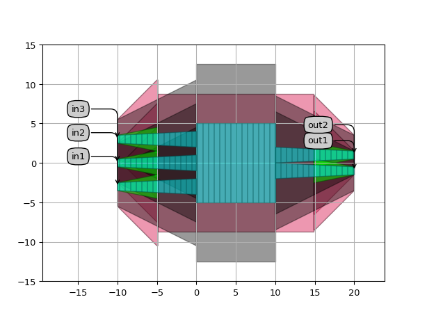
RibMMISymmetricTapered
- class picazzo3.filters.mmi_rib.RibMMISymmetricTapered
Rib MMI with symmetrically distributed access templates and with tapers.
- Parameters:
- output_trace_template: PCell
Output trace template.
- input_trace_template: PCell
Input trace template.
- mmi_trace_template: PCell and _WaveguideTemplate
Trace template used for the MMI section
- n_outputs: int and number > 0
Number of output channels.
- n_inputs: int and number > 0
Number of input channels
- trace_template: ( PCell and _WaveguideTemplate ), *None allowed*
Template for all ports, defaults to TECH.PCELLS.WG.DEFAULT.When set to None, the waveguide templates of the ports will be used.
- transition_database: AutoTransitionDatabase
AutoTransitionDatabase in which the correct transition between the two trace templates can be looked up.
- transitions: List with type restriction, allowed types: <class ‘ipkiss3.pcell.cell.pcell.PCell’>
List of transitions that is used on this MMI. By default Autotracetransition is used on all the transitions
- port_labels: ( List with type restriction, allowed types: <class ‘str’> ), *None allowed*
Labels of the ports to be processed. Set to None to process all ports.
- external_port_names: str
Dictionary for remapping of the port names of the contents to the external ports
- name: String that contains only ISO/IEC 8859-1 (extended ASCII py3) or pure ASCII (py2) characters
The unique name of the pcell
- Other Parameters:
- mmi_trace: PCell, locked
Trace of the MMI section
- output_trace_templates: List with type restriction, allowed types: <class ‘ipkiss3.pcell.cell.pcell.PCell’>, locked
List of the output trace templates.
- input_trace_templates: List with type restriction, allowed types: <class ‘ipkiss3.pcell.cell.pcell.PCell’>, locked
List of the input trace templates.
- trace_templates: List with type restriction, allowed types: <class ‘ipkiss3.pcell.cell.pcell.PCell’>, locked
list of templates to apply to all ports
- contents: PCell, locked
Contains the base MMI without the tapers
Views
- class Layout
- Parameters:
- trace_spacing: float and Real, number and number >= 0
Offset between the traces at the input and the output
- rib_cover_purpose: PatternPurpose
Drawing purpose for covering the mmi and rib-only part of the tapers
- extra_line_thickness: float and Real, number and number >= 0
Extra width added to minimum_space to calculate the width of the line correction (usually you do not have to modify this)
- minimum_space: float and number > 0
Minimum space between the tapers needed for the line corrections to be added (usually you do not have to modify this)
- transition_length: ( float and Real, number and number >= 0 ), *None allowed*
Length of the transition. Set to None to take the standard transition length.
- zero_length_if_identical: ( bool, bool_ or int )
uses a zero-length transition if the trace templates are identical
- flatten_transitions: ( bool, bool_ or int )
if true, flattens the transitions one level
- straight_extension: ( Coord2 and number >= 0 ), *None allowed*
Tuple: straight extensions of the transitions. Set to None to take the standard straight extensions
- length: float and number > 0
Length of the MMI
- contents_transformation: GenericNoDistortTransform
transformation to apply to the contents
- flatten_contents: ( bool, bool_ or int )
if True, it will insert the contents as elements in the layout, rather than as an Instance
- view_name: String that contains only alphanumeric characters from the ASCII set or contains _$. ASCII set is extended on PY3.
The name of the view
- Other Parameters:
- output_y_positions: list<Real, number>, locked
Positions in the y direction at the output where access waveguides are be added
- input_y_positions: list<Real, number>, locked
Positions in the y direction at the input where ports are be added
- transition_lengths: locked
Examples
import si_fab.all as pdk  # noqa: F401
from picazzo3.filters.mmi_rib.cell import RibMMISymmetricTapered
from picazzo3.traces.rib_wg import RibWaveguideTemplate
from picazzo3.traces.wire_wg.trace import WireWaveguideTemplate

mmi_trace_template = RibWaveguideTemplate()
mmi_trace_template.Layout(core_width=10.0, cladding_width=25.0)

mmi_wav_template = WireWaveguideTemplate()
mmi_wav_template.Layout(core_width=1.0, cladding_width=5.0)

mmi_access_template = RibWaveguideTemplate()
mmi_access_template.Layout(core_width=2.0, cladding_width=15.0)

MMI = RibMMISymmetricTapered(
    mmi_trace_template=mmi_trace_template,
    input_trace_template=mmi_access_template,
    output_trace_template=mmi_access_template,
    trace_template=mmi_wav_template,
    n_inputs=3,
    n_outputs=2,
)

layout = MMI.Layout(transition_length=5.0, length=10.0, trace_spacing=2.0)
layout.visualize(annotate=True)
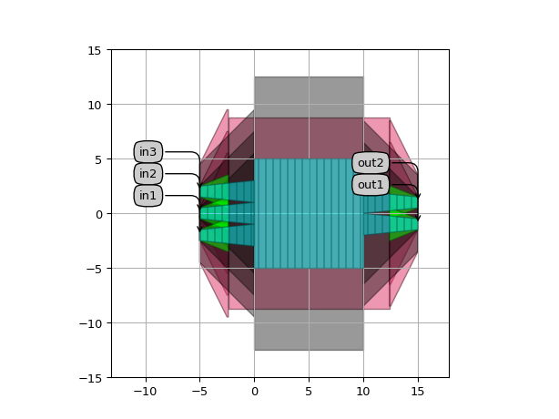
RibMMI1x2Tapered
- class picazzo3.filters.mmi_rib.RibMMI1x2Tapered
Rib 1x2 MMI with symmetrically distributed access templates and with tapers.
- Parameters:
- output_trace_template: PCell
Output trace template.
- input_trace_template: PCell
Input trace template.
- mmi_trace_template: PCell and _WaveguideTemplate
Trace template used for the MMI section
- trace_template: ( PCell and _WaveguideTemplate ), *None allowed*
Template for all ports, defaults to TECH.PCELLS.WG.DEFAULT.When set to None, the waveguide templates of the ports will be used.
- transition_database: AutoTransitionDatabase
AutoTransitionDatabase in which the correct transition between the two trace templates can be looked up.
- transitions: List with type restriction, allowed types: <class ‘ipkiss3.pcell.cell.pcell.PCell’>
List of transitions that is used on this MMI. By default Autotracetransition is used on all the transitions
- port_labels: ( List with type restriction, allowed types: <class ‘str’> ), *None allowed*
Labels of the ports to be processed. Set to None to process all ports.
- external_port_names: str
Dictionary for remapping of the port names of the contents to the external ports
- name: String that contains only ISO/IEC 8859-1 (extended ASCII py3) or pure ASCII (py2) characters
The unique name of the pcell
- Other Parameters:
- mmi_trace: PCell, locked
Trace of the MMI section
- output_trace_templates: List with type restriction, allowed types: <class ‘ipkiss3.pcell.cell.pcell.PCell’>, locked
List of the output trace templates.
- input_trace_templates: List with type restriction, allowed types: <class ‘ipkiss3.pcell.cell.pcell.PCell’>, locked
List of the input trace templates.
- n_outputs: int and number > 0, locked
Number of output channels.
- n_inputs: int and number > 0, locked
Number of input channels.
- trace_templates: List with type restriction, allowed types: <class ‘ipkiss3.pcell.cell.pcell.PCell’>, locked
list of templates to apply to all ports
- contents: PCell, locked
Contains the base MMI without the tapers
Views
- class Layout
- Parameters:
- trace_spacing: float and Real, number and number >= 0
Offset between the traces at the input and the output
- rib_cover_purpose: PatternPurpose
Drawing purpose for covering the mmi and rib-only part of the tapers
- extra_line_thickness: float and Real, number and number >= 0
Extra width added to minimum_space to calculate the width of the line correction (usually you do not have to modify this)
- minimum_space: float and number > 0
Minimum space between the tapers needed for the line corrections to be added (usually you do not have to modify this)
- transition_length: ( float and Real, number and number >= 0 ), *None allowed*
Length of the transition. Set to None to take the standard transition length.
- zero_length_if_identical: ( bool, bool_ or int )
uses a zero-length transition if the trace templates are identical
- flatten_transitions: ( bool, bool_ or int )
if true, flattens the transitions one level
- straight_extension: ( Coord2 and number >= 0 ), *None allowed*
Tuple: straight extensions of the transitions. Set to None to take the standard straight extensions
- length: float and number > 0
Length of the MMI
- contents_transformation: GenericNoDistortTransform
transformation to apply to the contents
- flatten_contents: ( bool, bool_ or int )
if True, it will insert the contents as elements in the layout, rather than as an Instance
- view_name: String that contains only alphanumeric characters from the ASCII set or contains _$. ASCII set is extended on PY3.
The name of the view
- Other Parameters:
- output_y_positions: list<Real, number>, locked
Positions in the y direction at the output where access waveguides are be added
- input_y_positions: list<Real, number>, locked
Positions in the y direction at the input where ports are be added
- transition_lengths: locked
Examples
import si_fab.all as pdk  # noqa: F401
from picazzo3.filters.mmi_rib.cell import RibMMI1x2Tapered
from picazzo3.traces.rib_wg import RibWaveguideTemplate
from picazzo3.traces.wire_wg.trace import WireWaveguideTemplate

mmi_trace_template = RibWaveguideTemplate()
mmi_trace_template.Layout(core_width=10.0, cladding_width=25.0)

mmi_wav_template = WireWaveguideTemplate()
mmi_wav_template.Layout(core_width=1.0, cladding_width=5.0)

mmi_access_template = RibWaveguideTemplate()
mmi_access_template.Layout(core_width=2.0, cladding_width=15.0)

MMI = RibMMI1x2Tapered(
    mmi_trace_template=mmi_trace_template,
    input_trace_template=mmi_access_template,
    output_trace_template=mmi_access_template,
    trace_template=mmi_wav_template,
)

layout = MMI.Layout(transition_length=5.0, length=10.0, trace_spacing=2.0)
layout.visualize(annotate=True)
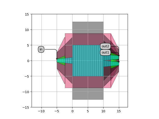
RibMMI2x1Tapered
- class picazzo3.filters.mmi_rib.RibMMI2x1Tapered
Rib 2x1 MMI with symmetrically distributed access templates and with tapers.
- Parameters:
- output_trace_template: PCell
Output trace template.
- input_trace_template: PCell
Input trace template.
- mmi_trace_template: PCell and _WaveguideTemplate
Trace template used for the MMI section
- trace_template: ( PCell and _WaveguideTemplate ), *None allowed*
Template for all ports, defaults to TECH.PCELLS.WG.DEFAULT.When set to None, the waveguide templates of the ports will be used.
- transition_database: AutoTransitionDatabase
AutoTransitionDatabase in which the correct transition between the two trace templates can be looked up.
- transitions: List with type restriction, allowed types: <class ‘ipkiss3.pcell.cell.pcell.PCell’>
List of transitions that is used on this MMI. By default Autotracetransition is used on all the transitions
- port_labels: ( List with type restriction, allowed types: <class ‘str’> ), *None allowed*
Labels of the ports to be processed. Set to None to process all ports.
- external_port_names: str
Dictionary for remapping of the port names of the contents to the external ports
- name: String that contains only ISO/IEC 8859-1 (extended ASCII py3) or pure ASCII (py2) characters
The unique name of the pcell
- Other Parameters:
- mmi_trace: PCell, locked
Trace of the MMI section
- output_trace_templates: List with type restriction, allowed types: <class ‘ipkiss3.pcell.cell.pcell.PCell’>, locked
List of the output trace templates.
- input_trace_templates: List with type restriction, allowed types: <class ‘ipkiss3.pcell.cell.pcell.PCell’>, locked
List of the input trace templates.
- n_outputs: int and number > 0, locked
Number of output channels.
- n_inputs: int and number > 0, locked
Number of input channels.
- trace_templates: List with type restriction, allowed types: <class ‘ipkiss3.pcell.cell.pcell.PCell’>, locked
list of templates to apply to all ports
- contents: PCell, locked
Contains the base MMI without the tapers
Views
- class Layout
- Parameters:
- trace_spacing: float and Real, number and number >= 0
Offset between the traces at the input and the output
- rib_cover_purpose: PatternPurpose
Drawing purpose for covering the mmi and rib-only part of the tapers
- extra_line_thickness: float and Real, number and number >= 0
Extra width added to minimum_space to calculate the width of the line correction (usually you do not have to modify this)
- minimum_space: float and number > 0
Minimum space between the tapers needed for the line corrections to be added (usually you do not have to modify this)
- transition_length: ( float and Real, number and number >= 0 ), *None allowed*
Length of the transition. Set to None to take the standard transition length.
- zero_length_if_identical: ( bool, bool_ or int )
uses a zero-length transition if the trace templates are identical
- flatten_transitions: ( bool, bool_ or int )
if true, flattens the transitions one level
- straight_extension: ( Coord2 and number >= 0 ), *None allowed*
Tuple: straight extensions of the transitions. Set to None to take the standard straight extensions
- length: float and number > 0
Length of the MMI
- contents_transformation: GenericNoDistortTransform
transformation to apply to the contents
- flatten_contents: ( bool, bool_ or int )
if True, it will insert the contents as elements in the layout, rather than as an Instance
- view_name: String that contains only alphanumeric characters from the ASCII set or contains _$. ASCII set is extended on PY3.
The name of the view
- Other Parameters:
- output_y_positions: list<Real, number>, locked
Positions in the y direction at the output where access waveguides are be added
- input_y_positions: list<Real, number>, locked
Positions in the y direction at the input where ports are be added
- transition_lengths: locked
Examples
import si_fab.all as pdk  # noqa: F401
from picazzo3.filters.mmi_rib.cell import RibMMI2x1Tapered
from picazzo3.traces.rib_wg import RibWaveguideTemplate
from picazzo3.traces.wire_wg.trace import WireWaveguideTemplate

mmi_trace_template = RibWaveguideTemplate()
mmi_trace_template.Layout(core_width=10.0, cladding_width=25.0)

mmi_wav_template = WireWaveguideTemplate()
mmi_wav_template.Layout(core_width=1.0, cladding_width=5.0)

mmi_access_template = RibWaveguideTemplate()
mmi_access_template.Layout(core_width=2.0, cladding_width=15.0)

MMI = RibMMI2x1Tapered(
    mmi_trace_template=mmi_trace_template,
    input_trace_template=mmi_access_template,
    output_trace_template=mmi_access_template,
    trace_template=mmi_wav_template,
)

layout = MMI.Layout(transition_length=5.0, length=10.0, trace_spacing=2.0)
layout.visualize(annotate=True)
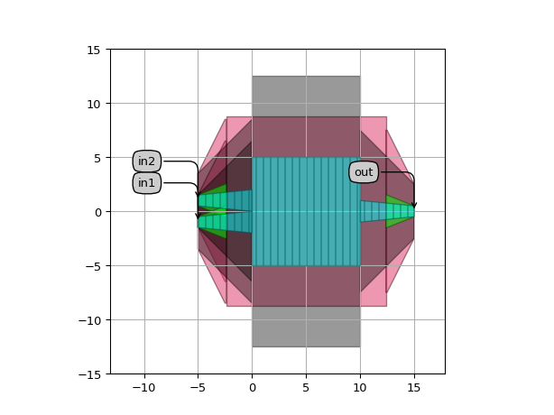
RibMMI2x2Tapered
- class picazzo3.filters.mmi_rib.RibMMI2x2Tapered
Rib 2x2 MMI with symmetrically distributed access templates and with tapers.
- Parameters:
- output_trace_template: PCell
Output trace template.
- input_trace_template: PCell
Input trace template.
- mmi_trace_template: PCell and _WaveguideTemplate
Trace template used for the MMI section
- trace_template: ( PCell and _WaveguideTemplate ), *None allowed*
Template for all ports, defaults to TECH.PCELLS.WG.DEFAULT.When set to None, the waveguide templates of the ports will be used.
- transition_database: AutoTransitionDatabase
AutoTransitionDatabase in which the correct transition between the two trace templates can be looked up.
- transitions: List with type restriction, allowed types: <class ‘ipkiss3.pcell.cell.pcell.PCell’>
List of transitions that is used on this MMI. By default Autotracetransition is used on all the transitions
- port_labels: ( List with type restriction, allowed types: <class ‘str’> ), *None allowed*
Labels of the ports to be processed. Set to None to process all ports.
- external_port_names: str
Dictionary for remapping of the port names of the contents to the external ports
- name: String that contains only ISO/IEC 8859-1 (extended ASCII py3) or pure ASCII (py2) characters
The unique name of the pcell
- Other Parameters:
- mmi_trace: PCell, locked
Trace of the MMI section
- output_trace_templates: List with type restriction, allowed types: <class ‘ipkiss3.pcell.cell.pcell.PCell’>, locked
List of the output trace templates.
- input_trace_templates: List with type restriction, allowed types: <class ‘ipkiss3.pcell.cell.pcell.PCell’>, locked
List of the input trace templates.
- n_outputs: int and number > 0, locked
Number of output channels.
- n_inputs: int and number > 0, locked
Number of input channels.
- trace_templates: List with type restriction, allowed types: <class ‘ipkiss3.pcell.cell.pcell.PCell’>, locked
list of templates to apply to all ports
- contents: PCell, locked
Contains the base MMI without the tapers
Views
- class Layout
- Parameters:
- trace_spacing: float and Real, number and number >= 0
Offset between the traces at the input and the output
- rib_cover_purpose: PatternPurpose
Drawing purpose for covering the mmi and rib-only part of the tapers
- extra_line_thickness: float and Real, number and number >= 0
Extra width added to minimum_space to calculate the width of the line correction (usually you do not have to modify this)
- minimum_space: float and number > 0
Minimum space between the tapers needed for the line corrections to be added (usually you do not have to modify this)
- transition_length: ( float and Real, number and number >= 0 ), *None allowed*
Length of the transition. Set to None to take the standard transition length.
- zero_length_if_identical: ( bool, bool_ or int )
uses a zero-length transition if the trace templates are identical
- flatten_transitions: ( bool, bool_ or int )
if true, flattens the transitions one level
- straight_extension: ( Coord2 and number >= 0 ), *None allowed*
Tuple: straight extensions of the transitions. Set to None to take the standard straight extensions
- length: float and number > 0
Length of the MMI
- contents_transformation: GenericNoDistortTransform
transformation to apply to the contents
- flatten_contents: ( bool, bool_ or int )
if True, it will insert the contents as elements in the layout, rather than as an Instance
- view_name: String that contains only alphanumeric characters from the ASCII set or contains _$. ASCII set is extended on PY3.
The name of the view
- Other Parameters:
- output_y_positions: list<Real, number>, locked
Positions in the y direction at the output where access waveguides are be added
- input_y_positions: list<Real, number>, locked
Positions in the y direction at the input where ports are be added
- transition_lengths: locked
Examples
import si_fab.all as pdk  # noqa: F401
from picazzo3.filters.mmi_rib.cell import RibMMI2x2Tapered
from picazzo3.traces.rib_wg import RibWaveguideTemplate
from picazzo3.traces.wire_wg.trace import WireWaveguideTemplate

mmi_trace_template = RibWaveguideTemplate()
mmi_trace_template.Layout(core_width=10.0, cladding_width=25.0)

mmi_wav_template = WireWaveguideTemplate()
mmi_wav_template.Layout(core_width=1.0, cladding_width=5.0)

mmi_access_template = RibWaveguideTemplate()
mmi_access_template.Layout(core_width=2.0, cladding_width=15.0)

MMI = RibMMI2x2Tapered(
    mmi_trace_template=mmi_trace_template,
    input_trace_template=mmi_access_template,
    output_trace_template=mmi_access_template,
    trace_template=mmi_wav_template,
)

layout = MMI.Layout(transition_length=5.0, length=10.0, trace_spacing=2.0)
layout.visualize(annotate=True)
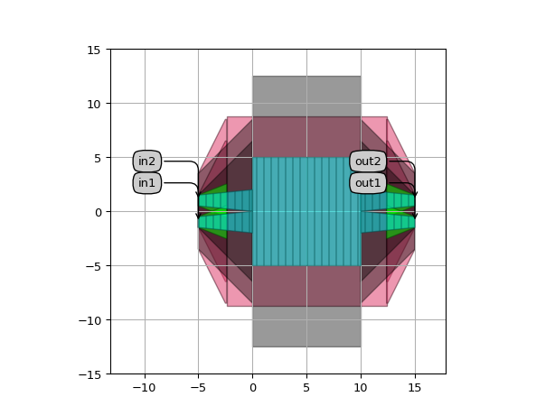
MMI
- class picazzo3.filters.mmi.MMI
Rectangular multimode interferometer, generated from a waveguide template
- Parameters:
- output_trace_templates: List with type restriction, allowed types: <class ‘ipkiss3.pcell.cell.pcell.PCell’>
List of the output trace templates.
- input_trace_templates: List with type restriction, allowed types: <class ‘ipkiss3.pcell.cell.pcell.PCell’>
List of the input trace templates.
- mmi_trace_template: PCell and _WaveguideTemplate
Trace template used for the MMI section
- name: String that contains only ISO/IEC 8859-1 (extended ASCII py3) or pure ASCII (py2) characters
The unique name of the pcell
- Other Parameters:
- mmi_trace: PCell, locked
Trace of the MMI section
- n_outputs: int and number > 0, locked
Number of output channels.
- n_inputs: int and number > 0, locked
Number of input channels.
Views
- class Layout
Layoutview of the MMI. It is built from the MMI waveguide over a certain length and ports at the input_y_positions and output_y_positions.
- Parameters:
- length: float and number > 0
Length of the MMI
- output_y_positions: list<Real, number>
Positions in the y direction at the output where ports are be added
- input_y_positions: list<Real, number>
Positions in the y direction at the input where ports are be added
- view_name: String that contains only alphanumeric characters from the ASCII set or contains _$. ASCII set is extended on PY3.
The name of the view
Examples
import si_fab.all as pdk  # noqa: F401
from ipkiss3 import all as i3
from picazzo3.filters.mmi.cell import MMI
from picazzo3.traces.wire_wg.trace import WireWaveguideTemplate

mmi_trace_template = WireWaveguideTemplate()
mmi_trace_template.Layout(core_width=6.0, cladding_width=10.0)
MMI = MMI(
    mmi_trace_template=mmi_trace_template,
    input_trace_templates=[i3.TECH.PCELLS.WG.DEFAULT],
    output_trace_templates=[i3.TECH.PCELLS.WG.DEFAULT],
)
layout = MMI.Layout(length=10.0, input_y_positions=[0.0], output_y_positions=[0.0])
layout.visualize(annotate=True)
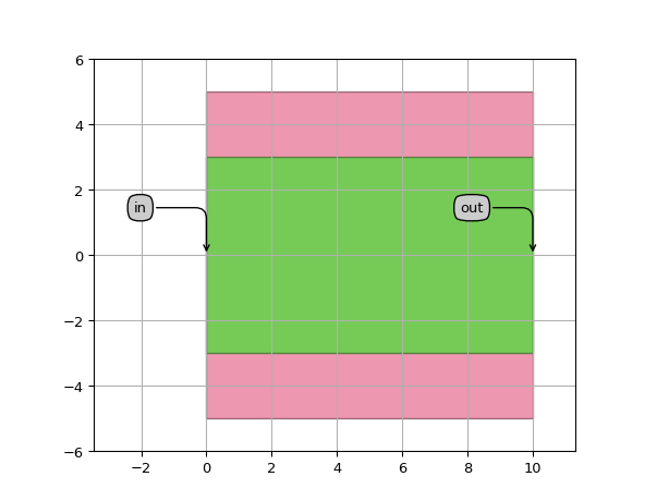
MMIIdentical
- class picazzo3.filters.mmi.MMIIdentical
Rectangular multimode interferometer, generated from a trace template with identical input and output trace_templates.
- Parameters:
- output_trace_template: PCell
Output trace template.
- input_trace_template: PCell
Input trace template.
- mmi_trace_template: PCell and _WaveguideTemplate
Trace template used for the MMI section
- n_outputs: int and number > 0
Number of output channels.
- n_inputs: int and number > 0
Number of input channels
- name: String that contains only ISO/IEC 8859-1 (extended ASCII py3) or pure ASCII (py2) characters
The unique name of the pcell
- Other Parameters:
- mmi_trace: PCell, locked
Trace of the MMI section
- output_trace_templates: List with type restriction, allowed types: <class ‘ipkiss3.pcell.cell.pcell.PCell’>, locked
List of the output trace templates.
- input_trace_templates: List with type restriction, allowed types: <class ‘ipkiss3.pcell.cell.pcell.PCell’>, locked
List of the input trace templates.
Views
- class Layout
- Parameters:
- length: float and number > 0
Length of the MMI
- output_y_positions: list<Real, number>
Positions in the y direction at the output where ports are be added
- input_y_positions: list<Real, number>
Positions in the y direction at the input where ports are be added
- view_name: String that contains only alphanumeric characters from the ASCII set or contains _$. ASCII set is extended on PY3.
The name of the view
Examples
import si_fab.all as pdk  # noqa: F401
from picazzo3.filters.mmi.cell import MMIIdentical
from picazzo3.traces.wire_wg.trace import WireWaveguideTemplate
import ipkiss3.all as i3

mmi_trace_template = WireWaveguideTemplate()
mmi_trace_template.Layout(core_width=6.0, cladding_width=10.0)
MMI = MMIIdentical(
    mmi_trace_template=mmi_trace_template,
    input_trace_template=i3.TECH.PCELLS.WG.DEFAULT,
    output_trace_template=i3.TECH.PCELLS.WG.DEFAULT,
    n_inputs=3,
    n_outputs=2,
)
layout = MMI.Layout(length=10.0, input_y_positions=[-2.0, 0.0, 2.0], output_y_positions=[-1.0, 1.0])
layout.visualize(annotate=True)
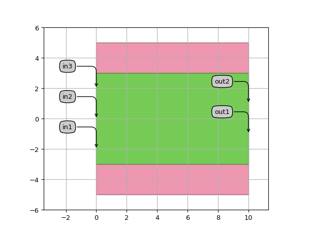
MMISymmetric
- class picazzo3.filters.mmi.MMISymmetric
MMI with symmetrically distributed access templates. This is usually useful when the MMI is used a splitter or combiner.
- Parameters:
- output_trace_template: PCell
Output trace template.
- input_trace_template: PCell
Input trace template.
- mmi_trace_template: PCell and _WaveguideTemplate
Trace template used for the MMI section
- n_outputs: int and number > 0
Number of output channels.
- n_inputs: int and number > 0
Number of input channels
- name: String that contains only ISO/IEC 8859-1 (extended ASCII py3) or pure ASCII (py2) characters
The unique name of the pcell
- Other Parameters:
- mmi_trace: PCell, locked
Trace of the MMI section
- output_trace_templates: List with type restriction, allowed types: <class ‘ipkiss3.pcell.cell.pcell.PCell’>, locked
List of the output trace templates.
- input_trace_templates: List with type restriction, allowed types: <class ‘ipkiss3.pcell.cell.pcell.PCell’>, locked
List of the input trace templates.
Views
- class Layout
- Parameters:
- trace_spacing: float and Real, number and number >= 0
Offset between the traces at the input and the output
- length: float and number > 0
Length of the MMI
- view_name: String that contains only alphanumeric characters from the ASCII set or contains _$. ASCII set is extended on PY3.
The name of the view
- Other Parameters:
- output_y_positions: list<Real, number>, locked
Positions in the y direction at the output where access waveguides are be added
- input_y_positions: list<Real, number>, locked
Positions in the y direction at the input where ports are be added
Examples
import si_fab.all as pdk  # noqa: F401
from picazzo3.filters.mmi.cell import MMISymmetric
from picazzo3.traces.wire_wg.trace import WireWaveguideTemplate
import ipkiss3.all as i3

mmi_trace_template = WireWaveguideTemplate()
mmi_trace_template.Layout(core_width=6.0, cladding_width=10.0)
MMI = MMISymmetric(
    mmi_trace_template=mmi_trace_template,
    input_trace_template=i3.TECH.PCELLS.WG.DEFAULT,
    output_trace_template=i3.TECH.PCELLS.WG.DEFAULT,
    n_inputs=3,
    n_outputs=2,
)
layout = MMI.Layout(length=10.0, trace_spacing=2.0)
layout.visualize(annotate=True)

MMI1x2
- class picazzo3.filters.mmi.MMI1x2
MMI with one access waveguide and two output waveguides that symmetrically distributed. This is usually useful when the MMI is used as a splitter.
- Parameters:
- output_trace_template: PCell
Output trace template.
- input_trace_template: PCell
Input trace template.
- mmi_trace_template: PCell and _WaveguideTemplate
Trace template used for the MMI section
- name: String that contains only ISO/IEC 8859-1 (extended ASCII py3) or pure ASCII (py2) characters
The unique name of the pcell
- Other Parameters:
- mmi_trace: PCell, locked
Trace of the MMI section
- output_trace_templates: List with type restriction, allowed types: <class ‘ipkiss3.pcell.cell.pcell.PCell’>, locked
List of the output trace templates.
- input_trace_templates: List with type restriction, allowed types: <class ‘ipkiss3.pcell.cell.pcell.PCell’>, locked
List of the input trace templates.
- n_outputs: int and number > 0, locked
Number of output channels.
- n_inputs: int and number > 0, locked
Number of input channels.
Views
- class Layout
- Parameters:
- trace_spacing: float and Real, number and number >= 0
Offset between the traces at the input and the output
- length: float and number > 0
Length of the MMI
- view_name: String that contains only alphanumeric characters from the ASCII set or contains _$. ASCII set is extended on PY3.
The name of the view
- Other Parameters:
- output_y_positions: list<Real, number>, locked
Positions in the y direction at the output where access waveguides are be added
- input_y_positions: list<Real, number>, locked
Positions in the y direction at the input where ports are be added
Examples
import si_fab.all as pdk  # noqa: F401
from picazzo3.filters.mmi.cell import MMI1x2
from picazzo3.traces.wire_wg.trace import WireWaveguideTemplate
import ipkiss3.all as i3

mmi_trace_template = WireWaveguideTemplate()
mmi_trace_template.Layout(core_width=6.0, cladding_width=10.0)
MMI = MMI1x2(
    mmi_trace_template=mmi_trace_template,
    input_trace_template=i3.TECH.PCELLS.WG.DEFAULT,
    output_trace_template=i3.TECH.PCELLS.WG.DEFAULT,
)
layout = MMI.Layout(length=10.0, trace_spacing=2.0)
layout.visualize(annotate=True)
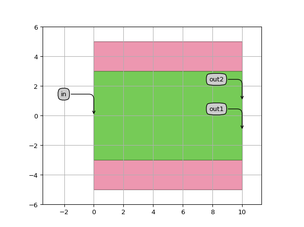
MMI2x1
- class picazzo3.filters.mmi.MMI2x1
MMI with two access waveguides and one output waveguides that symmetrically distributed. This is usually useful when the MMI is used as a combiner.
- Parameters:
- output_trace_template: PCell
Output trace template.
- input_trace_template: PCell
Input trace template.
- mmi_trace_template: PCell and _WaveguideTemplate
Trace template used for the MMI section
- name: String that contains only ISO/IEC 8859-1 (extended ASCII py3) or pure ASCII (py2) characters
The unique name of the pcell
- Other Parameters:
- mmi_trace: PCell, locked
Trace of the MMI section
- output_trace_templates: List with type restriction, allowed types: <class ‘ipkiss3.pcell.cell.pcell.PCell’>, locked
List of the output trace templates.
- input_trace_templates: List with type restriction, allowed types: <class ‘ipkiss3.pcell.cell.pcell.PCell’>, locked
List of the input trace templates.
- n_outputs: int and number > 0, locked
Number of output channels.
- n_inputs: int and number > 0, locked
Number of input channels.
Views
- class Layout
- Parameters:
- trace_spacing: float and Real, number and number >= 0
Offset between the traces at the input and the output
- length: float and number > 0
Length of the MMI
- view_name: String that contains only alphanumeric characters from the ASCII set or contains _$. ASCII set is extended on PY3.
The name of the view
- Other Parameters:
- output_y_positions: list<Real, number>, locked
Positions in the y direction at the output where access waveguides are be added
- input_y_positions: list<Real, number>, locked
Positions in the y direction at the input where ports are be added
Examples
import si_fab.all as pdk  # noqa: F401
from picazzo3.filters.mmi.cell import MMI2x1
from picazzo3.traces.wire_wg.trace import WireWaveguideTemplate
import ipkiss3.all as i3

mmi_trace_template = WireWaveguideTemplate()
mmi_trace_template.Layout(core_width=6.0, cladding_width=10.0)
MMI = MMI2x1(
    mmi_trace_template=mmi_trace_template,
    input_trace_template=i3.TECH.PCELLS.WG.DEFAULT,
    output_trace_template=i3.TECH.PCELLS.WG.DEFAULT,
)

layout = MMI.Layout(length=10.0, trace_spacing=2.0)
layout.visualize(annotate=True)
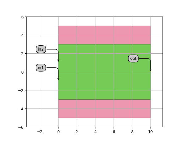
MMI2x2
- class picazzo3.filters.mmi.MMI2x2
MMI with one access waveguide and two output waveguides that symmetrically distributed. This is usually useful when the MMI is used as a 2x2 splitter or a crossing.
- Parameters:
- output_trace_template: PCell
Output trace template.
- input_trace_template: PCell
Input trace template.
- mmi_trace_template: PCell and _WaveguideTemplate
Trace template used for the MMI section
- name: String that contains only ISO/IEC 8859-1 (extended ASCII py3) or pure ASCII (py2) characters
The unique name of the pcell
- Other Parameters:
- mmi_trace: PCell, locked
Trace of the MMI section
- output_trace_templates: List with type restriction, allowed types: <class ‘ipkiss3.pcell.cell.pcell.PCell’>, locked
List of the output trace templates.
- input_trace_templates: List with type restriction, allowed types: <class ‘ipkiss3.pcell.cell.pcell.PCell’>, locked
List of the input trace templates.
- n_outputs: int and number > 0, locked
Number of output channels.
- n_inputs: int and number > 0, locked
Number of input channels.
Views
- class Layout
- Parameters:
- trace_spacing: float and Real, number and number >= 0
Offset between the traces at the input and the output
- length: float and number > 0
Length of the MMI
- view_name: String that contains only alphanumeric characters from the ASCII set or contains _$. ASCII set is extended on PY3.
The name of the view
- Other Parameters:
- output_y_positions: list<Real, number>, locked
Positions in the y direction at the output where access waveguides are be added
- input_y_positions: list<Real, number>, locked
Positions in the y direction at the input where ports are be added
Examples
import si_fab.all as pdk  # noqa: F401
from picazzo3.filters.mmi.cell import MMI2x2
from picazzo3.traces.wire_wg.trace import WireWaveguideTemplate
import ipkiss3.all as i3

mmi_trace_template = WireWaveguideTemplate()
mmi_trace_template.Layout(core_width=6.0, cladding_width=10.0)
MMI = MMI2x2(
    mmi_trace_template=mmi_trace_template,
    input_trace_template=i3.TECH.PCELLS.WG.DEFAULT,
    output_trace_template=i3.TECH.PCELLS.WG.DEFAULT,
)
layout = MMI.Layout(length=10.0, trace_spacing=2.0)
layout.visualize(annotate=True)
Mach-Zehnder Interferometers (MZI)
MZI
- class picazzo3.filters.mzi.cell.MZI
Generic MZI, taking a splitter, combiner and two _MziArm objects. You have to specify the transformations yourself.
- Parameters:
- arm2_port_names: String that contains only alphanumeric characters from the ASCII set or contains _$. ASCII set is extended on PY3. and length == 2
port names for the north arm ports connected to splitter and combiner. Default = (‘in’, ‘out’)
- arm1_port_names: String that contains only alphanumeric characters from the ASCII set or contains _$. ASCII set is extended on PY3. and length == 2
port names for the south arm ports connected to splitter and combiner. Default = (‘in’, ‘out’)
- combiner_port_names: String that contains only alphanumeric characters from the ASCII set or contains _$. ASCII set is extended on PY3. and length == 2
port names for the combiner ports to the arms. Default = (‘in1’, ‘in2’)
- splitter_port_names: String that contains only alphanumeric characters from the ASCII set or contains _$. ASCII set is extended on PY3. and length == 2
port names for the splitter ports to the arms. Default = (‘out1’, ‘out2’)
- combiner: PCell
The combiner of the MZI
- splitter: PCell
The splitter of the MZI
- arm2: PCell and MZIArm
The North arm of the MZI
- arm1: PCell and MZIArm
The South arm of the MZI
- external_port_names: str
Map of the free instance terms/ports to the names of external terms/ports.Format is a dict {‘inst:term’ : ‘new_term_name’}.If a term/port is not listed, the format instname_portname will be used
- name: String that contains only ISO/IEC 8859-1 (extended ASCII py3) or pure ASCII (py2) characters
The unique name of the pcell
- Other Parameters:
- links: locked
- child_cells: locked
Views
- class Layout
- Parameters:
- combiner_transformation: GenericNoDistortTransform
Transformation of the Combiner.
- splitter_transformation: GenericNoDistortTransform
Transformation of the Splitter.
- flyline_width: float and number > 0
line width of the flylines
- flyline_layer: ( __Layer__ ), *None allowed*
layer to draw flylines of physically unconnected links
- netlist_view: NetlistView
Netlist view in the same cell on which this Layout is based. Normally no need to manually override.
- view_name: String that contains only alphanumeric characters from the ASCII set or contains _$. ASCII set is extended on PY3.
The name of the view
- Other Parameters:
- child_transformations: locked
Examples
import si_fab.all as pdk  # noqa: F401
from picazzo3.filters.mzi import MZI, MZIWaveguideArm
from picazzo3.wg.splitters import WgY90Splitter
from picazzo3.traces.wire_wg.trace import WireWaveguideTemplate
from ipkiss3 import all as i3

wg1_t = WireWaveguideTemplate(name="my_wire_template_3")
wg1_t.Layout(core_width=0.5)

split = WgY90Splitter(name="my_splitter1")
split_layout = split.Layout()

comb_t = i3.HMirror() + i3.Translation((100.0, 0.0))

mziarm1 = MZIWaveguideArm(name="my_mzi_example_arm1")
mziarm1.Layout(
    extra_length=30.0,
    routing_direction=i3.DIRECTION.SOUTH,
    splitter_port=split_layout.ports["arm1"],
    combiner_port=split_layout.ports["arm1"].transform_copy(comb_t),
)

mziarm2 = MZIWaveguideArm(name="my_mzi_example_arm2")
mziarm2.Layout(
    splitter_port=split_layout.ports["arm2"],
    combiner_port=split_layout.ports["arm2"].transform_copy(comb_t),
)

mzi = MZI(
    name="my_mzi_example",
    splitter=split,
    combiner=split,
    arm1=mziarm1,
    arm2=mziarm2,
    splitter_port_names=["arm1", "arm2"],
    combiner_port_names=["arm1", "arm2"],
)
layout = mzi.Layout(combiner_transformation=comb_t)

layout.visualize(annotate=True)
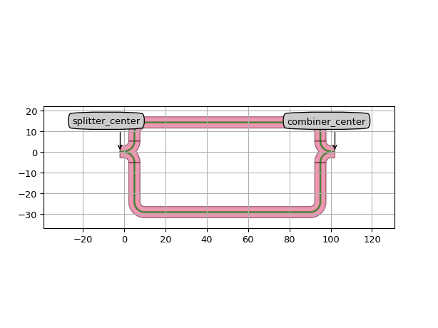
MZIWaveguides
- class picazzo3.filters.mzi.cell.MZIWaveguides
A MZI with two simple waveguide arms. The splitter and combiner are safely spaced, but this can be manually optimized. The difference in length between the delay lines can be set in the layout.
- Parameters:
- auto_transition: ( bool, bool_ or int )
if True, splitter and combiner are transitioned to the correct waveguide template
- trace_template: PCell and _WaveguideTemplate
- arm2_port_names: String that contains only alphanumeric characters from the ASCII set or contains _$. ASCII set is extended on PY3. and length == 2
port names for the north arm ports connected to splitter and combiner. Default = (‘in’, ‘out’)
- arm1_port_names: String that contains only alphanumeric characters from the ASCII set or contains _$. ASCII set is extended on PY3. and length == 2
port names for the south arm ports connected to splitter and combiner. Default = (‘in’, ‘out’)
- combiner_port_names: String that contains only alphanumeric characters from the ASCII set or contains _$. ASCII set is extended on PY3. and length == 2
port names for the combiner ports to the arms. Default = (‘in1’, ‘in2’)
- splitter_port_names: String that contains only alphanumeric characters from the ASCII set or contains _$. ASCII set is extended on PY3. and length == 2
port names for the splitter ports to the arms. Default = (‘out1’, ‘out2’)
- combiner: PCell
The combiner of the MZI
- splitter: PCell
The splitter of the MZI
- external_port_names: str
Map of the free instance terms/ports to the names of external terms/ports.Format is a dict {‘inst:term’ : ‘new_term_name’}.If a term/port is not listed, the format instname_portname will be used
- name: String that contains only ISO/IEC 8859-1 (extended ASCII py3) or pure ASCII (py2) characters
The unique name of the pcell
- Other Parameters:
- arm2: PCell, locked
- arm1: PCell, locked
- links: locked
- child_cells: locked
Views
- class Layout
- Parameters:
- delay_length: float
if positive, the upper arms is longer, if negative, the lower arm
- flatten_contents: ( bool, bool_ or int )
allows for enabling/disabling the flattening of the splitter and combiner, default is True
- min_straight: float and Real, number and number >= 0
Minimum straight length between two bends
- arm2_direction: List with value restriction, allowed values: [C2(0.000000, 1.000000), C2(0.000000, -1.000000)]
direction of routing (DIRECTION.NORTH or DIRECTION.SOUTH)
- arm1_direction: List with value restriction, allowed values: [C2(0.000000, 1.000000), C2(0.000000, -1.000000)]
direction of routing (DIRECTION.NORTH or DIRECTION.SOUTH)
- combiner_transformation: GenericNoDistortTransform
Transformation of the Combiner.
- splitter_transformation: GenericNoDistortTransform
Transformation of the Splitter.
- flyline_width: float and number > 0
line width of the flylines
- flyline_layer: ( __Layer__ ), *None allowed*
layer to draw flylines of physically unconnected links
- netlist_view: NetlistView
Netlist view in the same cell on which this Layout is based. Normally no need to manually override.
- view_name: String that contains only alphanumeric characters from the ASCII set or contains _$. ASCII set is extended on PY3.
The name of the view
- manhattan: ( bool, bool_ or int )
Adds rectangular blocks in the bends to avoid as much as possible non-manhattan angles.
- angle_step: float and number > 0
Angle step for rounding.
- rounding_algorithm:
Rounding algorithm used to generate the bends. Can be circular, spline, ….
- bend_radius: float and number > 0
Bend radius for the auto-generated bends.
- Other Parameters:
- child_transformations: locked
Examples
import si_fab.all as pdk  # noqa: F401
from picazzo3.filters.mzi import MZIWaveguides
from picazzo3.wg.splitters import WgY90Splitter, WgY180Combiner

split = WgY90Splitter(name="my_splitter_5")
split.Layout()

comb = WgY180Combiner(name="my_combiner_5")
comb.Layout()

mzi = MZIWaveguides(
    name="my_mzi_waveguides_1",
    splitter=split,
    combiner=comb,
    splitter_port_names=["arm1", "arm2"],
    combiner_port_names=["arm1", "arm2"],
)
layout = mzi.Layout(delay_length=100.0)

layout.visualize(annotate=True)
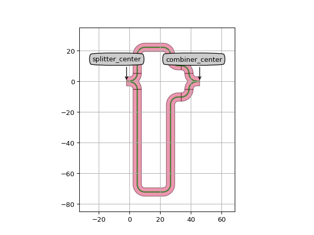
import si_fab.all as pdk  # noqa: F401
from picazzo3.filters.mzi import MZIWaveguides
from picazzo3.wg.dircoup import BendDirectionalCoupler
from ipkiss3 import all as i3

split = BendDirectionalCoupler(name="my_splitter_6")
split.Layout(bend_angle=30.0)

mzi = MZIWaveguides(name="my_mzi_waveguides_2", splitter=split, combiner=split)
layout = mzi.Layout(
    delay_length=-50.0,
    splitter_transformation=i3.Rotation(rotation=90.0),
    combiner_transformation=i3.Rotation(rotation=-90.0) + i3.Translation((25.0, 0.0)),
    arm1_direction=i3.DIRECTION.NORTH,
)

layout.visualize(annotate=True)
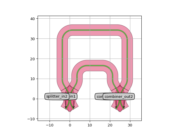
MZIWithCells
- class picazzo3.filters.mzi.cell.MZIWithCells
An MZI which contains another cell in one or both arms.
- Parameters:
- arm2_contents_port_names: String that contains only alphanumeric characters from the ASCII set or contains _$. ASCII set is extended on PY3. and length == 2
port names for the contents ports in arm2. Default = (‘in’, ‘out’)
- arm1_contents_port_names: String that contains only alphanumeric characters from the ASCII set or contains _$. ASCII set is extended on PY3. and length == 2
port names for the contents ports in arm1. Default = (‘in’, ‘out’)
- arm2_contents: ( PCell ), *None allowed*
Cell to place in the NORTH arm. Use None when only a waveguide is required.
- arm1_contents: ( PCell ), *None allowed*
Cell to place in the SOUTH arm. Use None when only a waveguide is required.
- auto_transition: ( bool, bool_ or int )
if True, splitter and combiner are transitioned to the correct waveguide template
- trace_template: PCell and _WaveguideTemplate
- arm2_port_names: String that contains only alphanumeric characters from the ASCII set or contains _$. ASCII set is extended on PY3. and length == 2
port names for the north arm ports connected to splitter and combiner. Default = (‘in’, ‘out’)
- arm1_port_names: String that contains only alphanumeric characters from the ASCII set or contains _$. ASCII set is extended on PY3. and length == 2
port names for the south arm ports connected to splitter and combiner. Default = (‘in’, ‘out’)
- combiner_port_names: String that contains only alphanumeric characters from the ASCII set or contains _$. ASCII set is extended on PY3. and length == 2
port names for the combiner ports to the arms. Default = (‘in1’, ‘in2’)
- splitter_port_names: String that contains only alphanumeric characters from the ASCII set or contains _$. ASCII set is extended on PY3. and length == 2
port names for the splitter ports to the arms. Default = (‘out1’, ‘out2’)
- combiner: PCell
The combiner of the MZI
- splitter: PCell
The splitter of the MZI
- arm2: PCell and MZIArm
The North arm of the MZI
- arm1: PCell and MZIArm
The South arm of the MZI
- external_port_names: str
Map of the free instance terms/ports to the names of external terms/ports.Format is a dict {‘inst:term’ : ‘new_term_name’}.If a term/port is not listed, the format instname_portname will be used
- name: String that contains only ISO/IEC 8859-1 (extended ASCII py3) or pure ASCII (py2) characters
The unique name of the pcell
- Other Parameters:
- links: locked
- child_cells: locked
Examples
import si_fab.all as pdk  # noqa: F401
from picazzo3.filters.mzi import MZIWithCells
from picazzo3.wg.dircoup import BendDirectionalCoupler
from picazzo3.filters.ring import RingRectNotchFilter

split = BendDirectionalCoupler(name="my_splitter_7")
split.Layout(bend_angle=30.0)

ring = RingRectNotchFilter(name="my_ring_8")

mzi = MZIWithCells(
    name="my_mzi_cells_1",
    splitter=split,
    combiner=split,
    arm1_contents=ring,
    arm1_contents_port_names=["in", "out"],
)
layout = mzi.Layout(extra_length=-50.0)

layout.visualize(annotate=True)
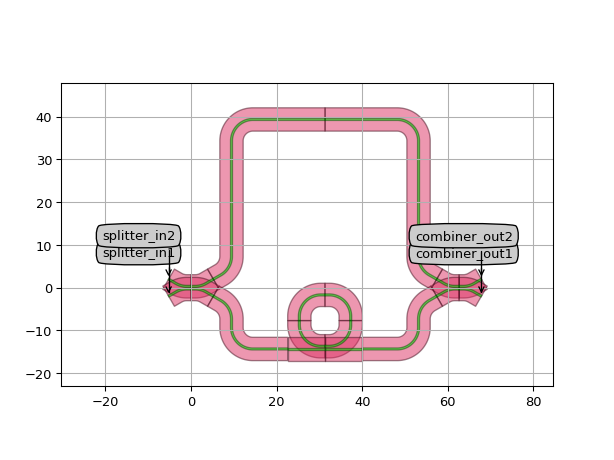
Views
- class Layout
- Parameters:
- arm2_contents_length: ( float and Real, number and number >= 0 ), *None allowed*
Specify manually the physical length of the content in the North arm. If None, it will be calculated by the arms from the distance between the ports.
- arm1_contents_length: ( float and Real, number and number >= 0 ), *None allowed*
Specify manually the physical length of the content in the South arm. If None, it will be calculated by the arms from the distance between the ports.
- arm2_contents_transformation: GenericNoDistortTransform
transformation of the contents in the North arm
- arm1_contents_transformation: GenericNoDistortTransform
transformation of the contents in the South arm
- extra_length: float
if positive, the lower (south) arm is longer, if negative, the upper (north) arm
- flatten_contents: ( bool, bool_ or int )
allows for enabling/disabling the flattening of the splitter and combiner, default is True
- min_straight: float and Real, number and number >= 0
Minimum straight length between two bends
- arm2_direction: List with value restriction, allowed values: [C2(0.000000, 1.000000), C2(0.000000, -1.000000)]
direction of routing (DIRECTION.NORTH or DIRECTION.SOUTH)
- arm1_direction: List with value restriction, allowed values: [C2(0.000000, 1.000000), C2(0.000000, -1.000000)]
direction of routing (DIRECTION.NORTH or DIRECTION.SOUTH)
- combiner_transformation: GenericNoDistortTransform
Transformation of the Combiner.
- splitter_transformation: GenericNoDistortTransform
Transformation of the Splitter.
- flyline_width: float and number > 0
line width of the flylines
- flyline_layer: ( __Layer__ ), *None allowed*
layer to draw flylines of physically unconnected links
- netlist_view: NetlistView
Netlist view in the same cell on which this Layout is based. Normally no need to manually override.
- view_name: String that contains only alphanumeric characters from the ASCII set or contains _$. ASCII set is extended on PY3.
The name of the view
- manhattan: ( bool, bool_ or int )
Adds rectangular blocks in the bends to avoid as much as possible non-manhattan angles.
- angle_step: float and number > 0
Angle step for rounding.
- rounding_algorithm:
Rounding algorithm used to generate the bends. Can be circular, spline, ….
- bend_radius: float and number > 0
Bend radius for the auto-generated bends.
- Other Parameters:
- child_transformations: locked
MZIWaveguideArm
- class picazzo3.filters.mzi.cell.MZIWaveguideArm
A Mach-Zehnder arm with a given length: routing upward at right-angle
- Parameters:
- trace_template: PCell and _WaveguideTemplate
- external_port_names: str
Dictionary for remapping of the port names of the contents to the external ports
- name: String that contains only ISO/IEC 8859-1 (extended ASCII py3) or pure ASCII (py2) characters
The unique name of the pcell
- Other Parameters:
- contents: PCell and _Trace, locked
Views
- class Layout
- Parameters:
- extra_length: float and Real, number and number >= 0
Extra length that will be added in the arm
- min_straight: float and Real, number and number >= 0
Minimum straight length between bends
- routing_direction: List with value restriction, allowed values: [C2(0.000000, 1.000000), C2(0.000000, -1.000000)]
direction of routing (DIRECTION.NORTH or DIRECTION.SOUTH)
- combiner_port: OpticalPort
Port interface of the combiner to which the output of this arm is connected
- splitter_port: OpticalPort
Port interface of the splitter to which the input of this arm is connected
- output_port: TracePort
- trace_template_for_ports: _TraceTemplate.Layout
Trace template to be used for the ports.
- cover_layers: List with type restriction, allowed types: <class ‘ipkiss.primitives.layer.Layer’>
layers that can be used to generate additional coverage of the trace (e.g. manhattan corners)
- reverse_individual_bends: list<( bool, bool_ or int )>
When set to True, it will generate the individual bends backwards. This has only effect when the bend algorithm is not symmetric. Should have length equal to the shape for closed shapes, but equal to shape-2 for open shapes.
- rounding_algorithms:
Rounding algorithm for every individual bend. Can be circular, spline, … Should have length equal to the shape for closed shapes, but equal to shape-2 for open shapes.
- bend_radii: list<number > 0>
Bend radius for every individual bend.
- reverse_bends: ( bool, bool_ or int )
When set to True, it will generate the bends backwards. This has only effect when the bend algorithm is not symmetric.
- remove_straight_angles: ( bool, bool_ or int )
Removes the waypoints with straight angles. Set to False if the algorithm uses waypoint-specific information.
- core_layer: __Layer__
layer used to define the core of the waveguide
- input_port: TracePort
- control_shape_layer: __Layer__
layer on which the control shape is drawn
- draw_control_shape: ( bool, bool_ or int )
draws the control shape on top of the waveguide
- contents_transformation: GenericNoDistortTransform
transformation to apply to the contents
- flatten_contents: ( bool, bool_ or int )
if True, it will insert the contents as elements in the layout, rather than as an Instance
- view_name: String that contains only alphanumeric characters from the ASCII set or contains _$. ASCII set is extended on PY3.
The name of the view
- manhattan: ( bool, bool_ or int )
Adds rectangular blocks in the bends to avoid as much as possible non-manhattan angles.
- angle_step: float and number > 0
Angle step for rounding.
- rounding_algorithm:
Rounding algorithm used to generate the bends. Can be circular, spline, ….
- bend_radius: float and number > 0
Bend radius for the auto-generated bends.
- Other Parameters:
- shape: locked
- center_line_shape: locked
Automatically calculated shape of the center line of the trace
Examples
import si_fab.all as pdk  # noqa: F401
from ipkiss3 import all as i3
from picazzo3.filters.mzi import MZIWaveguideArm
from picazzo3.traces.wire_wg.trace import WireWaveguideTemplate

wg1_t = WireWaveguideTemplate(name="my_template1")
wg1_t.Layout(core_width=0.5)

mziarm = MZIWaveguideArm(name="my_mziarm_1")
layout = mziarm.Layout(
    extra_length=30.0,
    splitter_port=i3.OpticalPort(position=(0.0, 0.0), angle_deg=30.0, trace_template=wg1_t),
    combiner_port=i3.OpticalPort(position=(40.0, 5.0), angle_deg=120.0, trace_template=wg1_t),
)

layout.visualize(annotate=True)
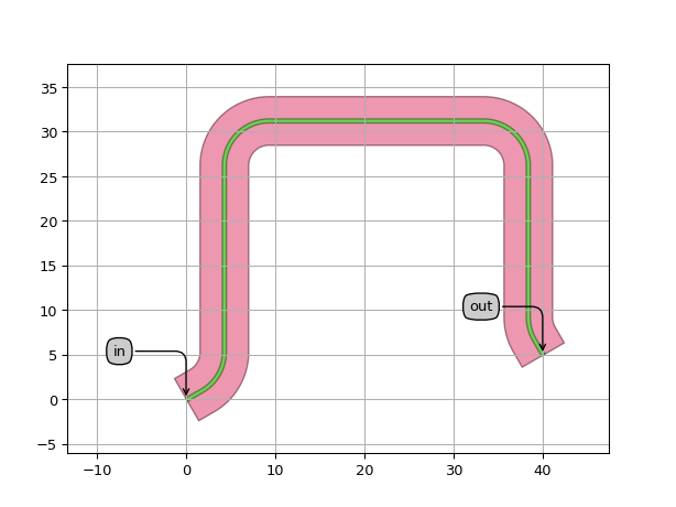
MZIContainerArm
- class picazzo3.filters.mzi.cell.MZIContainerArm
A Mach-Zehnder arm which contains another cell and connects it to the splitter and combiner port
- Parameters:
- trace_template: ( PCell and _WaveguideTemplate ), *None allowed*
Template for all ports, defaults to TECH.PCELLS.WG.DEFAULT.When set to None, the waveguide templates of the ports will be used.
- auto_transition: ( bool, bool_ or int )
if True, Automatic transitions will be added to the contents if the trace templates are not matched
- port_labels: List with type restriction, allowed types: <class ‘str’> and length == 2
Names of the two ports to be processed
- external_port_names: str
Dictionary for remapping of the port names of the contents to the external ports
- contents: PCell
the contents of the container: the child cell
- name: String that contains only ISO/IEC 8859-1 (extended ASCII py3) or pure ASCII (py2) characters
The unique name of the pcell
- Other Parameters:
- waveguides: List with type restriction, allowed types: <class ‘ipkiss3.pcell.cell.pcell.PCell’>, locked
- trace_templates: List with type restriction, allowed types: <class ‘ipkiss3.pcell.cell.pcell.PCell’>, locked
list of templates to apply to all ports
Views
- class Layout
- Parameters:
- contents_length: float and Real, number and number >= 0
The physical length of the optical path of the content. If not set manually, it will default to the distance between the content ports used.
- horizontal_contents_offset: float
Horizontal offset (from the center of the MZI Arm) of the transformed content
- extra_length: float and Real, number and number >= 0
Extra length that will be added in the arm
- min_straight: float and Real, number and number >= 0
Minimum straight length between bends
- combiner_port: OpticalPort
Port interface of the combiner to which the output of this arm is connected
- splitter_port: OpticalPort
Port interface of the splitter to which the input of this arm is connected
- routes:
routes along which the waveguides will be generated
- routing_direction: List with value restriction, allowed values: [C2(0.000000, 1.000000), C2(0.000000, -1.000000)]
direction of routing (DIRECTION.NORTH or DIRECTION.SOUTH)
- contents_transformation: GenericNoDistortTransform
transformation to apply to the contents
- flatten_contents: ( bool, bool_ or int )
if True, it will insert the contents as elements in the layout, rather than as an Instance
- view_name: String that contains only alphanumeric characters from the ASCII set or contains _$. ASCII set is extended on PY3.
The name of the view
- manhattan: ( bool, bool_ or int )
Adds rectangular blocks in the bends to avoid as much as possible non-manhattan angles.
- angle_step: float and number > 0
Angle step for rounding.
- rounding_algorithm:
Rounding algorithm used to generate the bends. Can be circular, spline, ….
- bend_radius: float and number > 0
Bend radius for the auto-generated bends.
Examples
import si_fab.all as pdk  # noqa: F401
from picazzo3.filters.mzi import MZIContainerArm
from picazzo3.filters.ring import RingRect180DropFilter
import ipkiss3.all as i3

ring = RingRect180DropFilter(name="my_ring_in_the_mzi_arm1")
ring.Layout(bend_radius=10.0)

mziarm = MZIContainerArm(name="my_mzi_container_arm", contents=ring, port_labels=["in1", "out1"])

layout = mziarm.Layout(
    extra_length=30.0,
    splitter_port=i3.OpticalPort(position=(0.0, 0.0), angle_deg=30.0),
    combiner_port=i3.OpticalPort(position=(60.0, 5.0), angle_deg=120.0),
    contents_transformation=i3.Rotation(rotation=30.0),
)
layout.visualize(annotate=True)
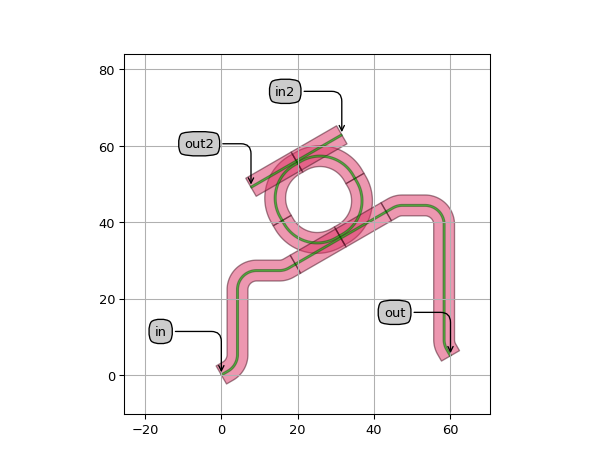
import si_fab.all as pdk  # noqa: F401
from picazzo3.filters.mzi import MZIContainerArm
from picazzo3.filters.ring import RingRect180DropFilter
import ipkiss3.all as i3

ring = RingRect180DropFilter(name="my_ring_in_the_mzi_arm2")
ring.Layout(bend_radius=10.0)

mziarm = MZIContainerArm(name="my_mzi_container_arm2", contents=ring, port_labels=["out2", "out1"])

layout = mziarm.Layout(
    extra_length=30.0,
    splitter_port=i3.OpticalPort(position=(0.0, 0.0), angle_deg=30.0),
    combiner_port=i3.OpticalPort(position=(80.0, 5.0), angle_deg=120.0),
    contents_transformation=i3.Rotation(rotation=30.0),
    routing_direction=i3.DIRECTION.SOUTH,
)
layout.visualize(annotate=True)
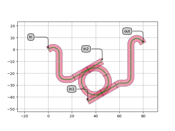
import si_fab.all as pdk  # noqa: F401
from picazzo3.filters.mzi import MZIContainerArm
from picazzo3.filters.ring import RingRect180DropFilter
import ipkiss3.all as i3

ring = RingRect180DropFilter(name="my_ring_in_the_mzi_arm3")
ring.Layout(bend_radius=10.0)

mziarm = MZIContainerArm(name="my_mzi_container_arm3", contents=ring, port_labels=["in1", "out1"])

layout = mziarm.Layout(
    extra_length=0.0,
    splitter_port=i3.OpticalPort(position=(0.0, 0.0), angle_deg=30.0),
    combiner_port=i3.OpticalPort(position=(30.0, 5.0), angle_deg=120.0),
    contents_transformation=i3.Rotation(rotation=30.0),
)
layout.visualize(annotate=True)
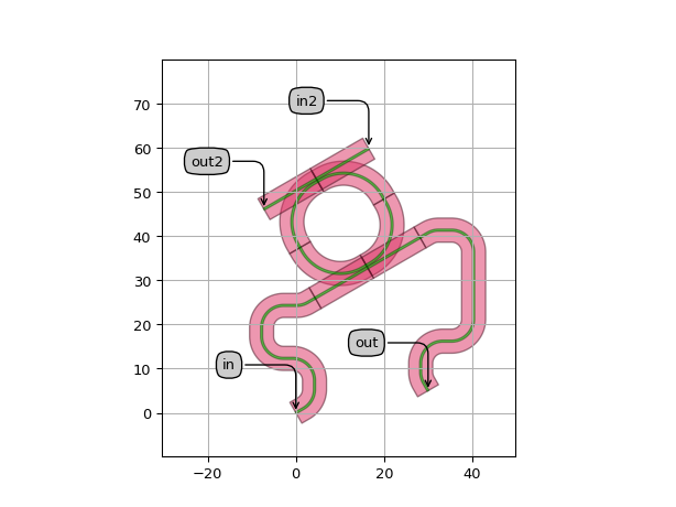
Photonic Crystals
Generic Photonic Crystals
DodecPhCLayout
- class picazzo3.phc.generic.cell.DodecPhCLayout
Generic Layouting Cell for photonic crystals with 12-sided holes on a Triangular lattice. The Layout of the cell is made up of a map, which is a multiline string representing the unit cells on a regular triangular lattice. The letters in the ‘map’ correspond to the diameters of the holes in the dictionary ‘hole_sizes’. The pitches can be defined as cartesian pitches using the property ‘pitches’, or using the property ‘lattice_pitches’ which specifies the lattice vector along the horizontal and the oblique axis, or using the property ‘pitch’, which just sets a uniform pitch along all lattice vectors.
- Parameters:
- name: String that contains only ISO/IEC 8859-1 (extended ASCII py3) or pure ASCII (py2) characters
The unique name of the pcell
See also
Views
- class Layout
- Parameters:
- purpose: PatternPurpose
Purpose of the layer on which the holes should be drawn.
- process_wg: ProcessLayer
Process of the layer on which the holes should be drawn.
- hole_sizes: dict
dictionary of the hole sizes of the Photonic Crystal. The value should be of the form {‘x’: 0.25, ‘y’: 0.26}. The keys of the dictionary should be characters and each character can be used to identify the unit cell in the map. If the property ‘cells’ is set manually, hole_sizes’ will be ignored.
- pitch: float and Real, number and number >= 0
Lattice constant for a uniform triangular lattice. This property will be ignored if ‘lattice_pitches’ or ‘pitches’ are set manually
- lattice_pitches: Coord2 and number >= 0
Lattice constants along the horizontal and the oblique direction. Choose identical values for a regular grid. If ‘pitches’ is manually set, this property will be ignored. If this property is set, the property ‘pitch’ will be ignored.
- ports_coordinates:
list of tuple with (coordinate (in pitches), angle, waveguide_template, [name])
- zero_line_y: float
line in the map which corresponds to the coordinate y=0. This can be a fractional number, and the unit is relative to pitches.y .
- purpose_hfw: PatternPurpose
drawing purpose for underetching
- process_hfw: ProcessLayer
process for underetching
- map: str and String that contains only ISO/IEC 8859-1 (extended ASCII py3) or pure ASCII (py2) characters
Map of the photonic crystal. This property accepts a multi-line string. Every character in the string represents a unit cell of the photonic crystal, which can be found in the property cells
- cells:
dictionary of Unit Cells for a Photonic Crystal. The value should be of the form {‘x’: cell1, ‘y’: cell2}. The keys of the dictionary should be characters and each character can be used to identify the unit cell in the map. The default value of this property is automatically calculated from the dictionary ‘hole_sizes’. Only assign to this property if you want to override this value. If you do this, the property ‘hole_sizes’ will be ignored.
- pitches:
Cartesian (X, Y) pitches of the lattice. If this is specified, the properties ‘lattice_pitches’ and ‘pitch’ will be ignored
- view_name: String that contains only alphanumeric characters from the ASCII set or contains _$. ASCII set is extended on PY3.
The name of the view
Examples
import si_fab.all as pdk  # noqa: F401
from ipkiss3 import all as i3

TECH = i3.TECH
from picazzo3.phc.generic import DodecPhCLayout

my_phc_map = [
    "A A A A A A A A A A A",
    " B   A A A A A A   B",
    "A B   A A   A A   B A",
    " A B   A     A   B A",
    "A A B     B     B A A",
    " A A B   B B   B A A",
    "A A A B B A B B A A A",
    " A A A B A A B A A A",
    "A A A A A A A A A A A",
]  # a W-shaped cavity
cell = DodecPhCLayout(name="my_dodec_phc_layout1")
layout = cell.Layout(
    pitch=0.45,
    hole_sizes={"A": 0.290, "B": 0.190},  # two sizes
    map="\n".join(my_phc_map),
    zero_line_y=5,  # count lines from the top
    ports_coordinates=[
        ((-0.5, 0), 180, TECH.PCELLS.WG.DEFAULT),
        ((10.5, 0), 0, TECH.PCELLS.WG.DEFAULT),
    ],  # coordinates expressed in lattice pitches
)

layout.visualize(annotate=True)
HexPhCLayout
- class picazzo3.phc.generic.cell.HexPhCLayout
Generic Layouting Cell for photonic crystals with hexagon holes on a Triangular lattice. The Layout of the cell is made up of a map, which is a multiline string representing the unit cells on a regular triangular lattice. The letters in the ‘map’ correspond to the diameters of the holes in the dictionary ‘hole_sizes’. The pitches can be defined as cartesian pitches using the property ‘pitches’, or using the property ‘lattice_pitches’ which specifies the lattice vector along the horizontal and the oblique axis, or using the property ‘pitch’, which just sets a uniform pitch along all lattice vectors.
- Parameters:
- name: String that contains only ISO/IEC 8859-1 (extended ASCII py3) or pure ASCII (py2) characters
The unique name of the pcell
See also
Views
- class Layout
- Parameters:
- purpose: PatternPurpose
Purpose of the layer on which the holes should be drawn.
- process_wg: ProcessLayer
Process of the layer on which the holes should be drawn.
- hole_sizes: dict
dictionary of the hole sizes of the Photonic Crystal. The value should be of the form {‘x’: 0.25, ‘y’: 0.26}. The keys of the dictionary should be characters and each character can be used to identify the unit cell in the map. If the property ‘cells’ is set manually, hole_sizes’ will be ignored.
- pitch: float and Real, number and number >= 0
Lattice constant for a uniform triangular lattice. This property will be ignored if ‘lattice_pitches’ or ‘pitches’ are set manually
- lattice_pitches: Coord2 and number >= 0
Lattice constants along the horizontal and the oblique direction. Choose identical values for a regular grid. If ‘pitches’ is manually set, this property will be ignored. If this property is set, the property ‘pitch’ will be ignored.
- ports_coordinates:
list of tuple with (coordinate (in pitches), angle, waveguide_template, [name])
- zero_line_y: float
line in the map which corresponds to the coordinate y=0. This can be a fractional number, and the unit is relative to pitches.y .
- purpose_hfw: PatternPurpose
drawing purpose for underetching
- process_hfw: ProcessLayer
process for underetching
- map: str and String that contains only ISO/IEC 8859-1 (extended ASCII py3) or pure ASCII (py2) characters
Map of the photonic crystal. This property accepts a multi-line string. Every character in the string represents a unit cell of the photonic crystal, which can be found in the property cells
- cells:
dictionary of Unit Cells for a Photonic Crystal. The value should be of the form {‘x’: cell1, ‘y’: cell2}. The keys of the dictionary should be characters and each character can be used to identify the unit cell in the map. The default value of this property is automatically calculated from the dictionary ‘hole_sizes’. Only assign to this property if you want to override this value. If you do this, the property ‘hole_sizes’ will be ignored.
- pitches:
Cartesian (X, Y) pitches of the lattice. If this is specified, the properties ‘lattice_pitches’ and ‘pitch’ will be ignored
- view_name: String that contains only alphanumeric characters from the ASCII set or contains _$. ASCII set is extended on PY3.
The name of the view
Examples
import si_fab.all as pdk  # noqa: F401
from ipkiss3 import all as i3

TECH = i3.TECH
from picazzo3.phc.generic import HexPhCLayout

my_phc_map = [
    "A A A A A A A A A A A",
    " B   A A A A A A   B",
    "A B   A A   A A   B A",
    " A B   A     A   B A",
    "A A B     B     B A A",
    " A A B   B B   B A A",
    "A A A B B A B B A A A",
    " A A A B A A B A A A",
    "A A A A A A A A A A A",
]  # a W-shaped cavity
cell = HexPhCLayout(name="my_hex_phc_layout1")
layout = cell.Layout(
    pitch=0.45,
    hole_sizes={"A": 0.290, "B": 0.190},  # two sizes
    map="\n".join(my_phc_map),
    zero_line_y=5,  # count lines from the top
    ports_coordinates=[
        ((-0.5, 0), 180, TECH.PCELLS.WG.DEFAULT),
        ((10.5, 0), 0, TECH.PCELLS.WG.DEFAULT),
    ],  # coordinates expressed in lattice pitches
)

layout.visualize(annotate=True)
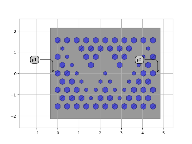
OctPhCLayout
- class picazzo3.phc.generic.cell.OctPhCLayout
Generic Layouting cell for Photonic Crystals with octagon holes on a Rectangular lattice. The Layout of the cell is made up of a map, which is a multiline string representing the unit cells on a regular rectangular lattice. The letters in the ‘map’ correspond to the diameters of the holes in the dictionary ‘hole_sizes’.
- Parameters:
- name: String that contains only ISO/IEC 8859-1 (extended ASCII py3) or pure ASCII (py2) characters
The unique name of the pcell
See also
Views
- class Layout
- Parameters:
- process_wg: ProcessLayer
Process of the layer on which the holes should be drawn.
- hole_sizes: dict
dictionary of the hole sizes of the Photonic Crystal. The value should be of the form {‘x’: 0.25, ‘y’: 0.26}. The keys of the dictionary should be characters and each character can be used to identify the unit cell in the map. If the property ‘cells’ is set manually, hole_sizes’ will be ignored.
- purpose: PatternPurpose
Purpose of the layer on which the holes should be drawn.
- pitch: float and Real, number and number >= 0
Lattice constant for a uniform square lattice. This property will be ignored if the property ‘pitches’ is set manually
- ports_coordinates:
list of tuple with (coordinate (in pitches), angle, waveguide_template, [name])
- zero_line_y: float
line in the map which corresponds to the coordinate y=0. This can be a fractional number, and the unit is relative to pitches.y .
- purpose_hfw: PatternPurpose
drawing purpose for underetching
- process_hfw: ProcessLayer
process for underetching
- map: str and String that contains only ISO/IEC 8859-1 (extended ASCII py3) or pure ASCII (py2) characters
Map of the photonic crystal. This property accepts a multi-line string. Every character in the string represents a unit cell of the photonic crystal, which can be found in the property cells
- cells:
dictionary of Unit Cells for a Photonic Crystal. The value should be of the form {‘x’: cell1, ‘y’: cell2}. The keys of the dictionary should be characters and each character can be used to identify the unit cell in the map. The default value of this property is automatically calculated from the dictionary ‘hole_sizes’. Only assign to this property if you want to override this value. If you do this, the property ‘hole_sizes’ will be ignored.
- pitches: Coord2 and number >= 0
X and Y pitch of the photonic crystal
- view_name: String that contains only alphanumeric characters from the ASCII set or contains _$. ASCII set is extended on PY3.
The name of the view
Examples
import si_fab.all as pdk  # noqa: F401
from ipkiss3 import all as i3

TECH = i3.TECH
from picazzo3.phc.generic import OctPhCLayout

my_phc_map = ["AAAAAAAA", "AAAAAAAA", "AA AA AA", "BBBAABBB", "AAAAAAAA"]
cell = OctPhCLayout(name="my_oct_phc_layout1")
layout = cell.Layout(
    pitch=0.45,
    hole_sizes={"A": 0.290, "B": 0.190},  # two sizes
    map="\n".join(my_phc_map),
    zero_line_y=5,  # count lines from the top
    ports_coordinates=[
        ((-0.5, 0), 180, TECH.PCELLS.WG.DEFAULT),
        ((10.5, 0), 0, TECH.PCELLS.WG.DEFAULT),
    ],  # coordinates expressed in lattice pitches
)

layout.visualize(annotate=True)
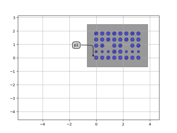
SquarePhCLayout
- class picazzo3.phc.generic.cell.SquarePhCLayout
Generic Layouting cell for Photonic Crystals with square holes on a Rectangular lattice. The Layout of the cell is made up of a map, which is a multiline string representing the unit cells on a regular rectangular lattice. The letters in the ‘map’ correspond to the diameters of the holes in the dictionary ‘hole_sizes’.
- Parameters:
- name: String that contains only ISO/IEC 8859-1 (extended ASCII py3) or pure ASCII (py2) characters
The unique name of the pcell
See also
Views
- class Layout
- Parameters:
- process_wg: ProcessLayer
Process of the layer on which the holes should be drawn.
- hole_sizes: dict
dictionary of the hole sizes of the Photonic Crystal. The value should be of the form {‘x’: 0.25, ‘y’: 0.26}. The keys of the dictionary should be characters and each character can be used to identify the unit cell in the map. If the property ‘cells’ is set manually, hole_sizes’ will be ignored.
- purpose: PatternPurpose
Purpose of the layer on which the holes should be drawn.
- pitch: float and Real, number and number >= 0
Lattice constant for a uniform square lattice. This property will be ignored if the property ‘pitches’ is set manually
- ports_coordinates:
list of tuple with (coordinate (in pitches), angle, waveguide_template, [name])
- zero_line_y: float
line in the map which corresponds to the coordinate y=0. This can be a fractional number, and the unit is relative to pitches.y .
- purpose_hfw: PatternPurpose
drawing purpose for underetching
- process_hfw: ProcessLayer
process for underetching
- map: str and String that contains only ISO/IEC 8859-1 (extended ASCII py3) or pure ASCII (py2) characters
Map of the photonic crystal. This property accepts a multi-line string. Every character in the string represents a unit cell of the photonic crystal, which can be found in the property cells
- cells:
dictionary of Unit Cells for a Photonic Crystal. The value should be of the form {‘x’: cell1, ‘y’: cell2}. The keys of the dictionary should be characters and each character can be used to identify the unit cell in the map. The default value of this property is automatically calculated from the dictionary ‘hole_sizes’. Only assign to this property if you want to override this value. If you do this, the property ‘hole_sizes’ will be ignored.
- pitches: Coord2 and number >= 0
X and Y pitch of the photonic crystal
- view_name: String that contains only alphanumeric characters from the ASCII set or contains _$. ASCII set is extended on PY3.
The name of the view
Examples
import si_fab.all as pdk  # noqa: F401
from ipkiss3 import all as i3

TECH = i3.TECH
from picazzo3.phc.generic import SquarePhCLayout

my_phc_map = ["AAAAAAAA", "AAAAAAAA", "AA AA AA", "BBBAABBB", "AAAAAAAA"]
cell = SquarePhCLayout(name="my_square_phc_layout1")
layout = cell.Layout(
    pitch=0.45,
    hole_sizes={"A": 0.290, "B": 0.190},  # two sizes
    map="\n".join(my_phc_map),
    zero_line_y=5,  # count lines from the top
    ports_coordinates=[
        ((-0.5, 0), 180, TECH.PCELLS.WG.DEFAULT),
        ((10.5, 0), 0, TECH.PCELLS.WG.DEFAULT),
    ],  # coordinates expressed in lattice pitches
)

layout.visualize(annotate=True)

TriangularPhCLayout
- class picazzo3.phc.generic.cell.TriangularPhCLayout
Generic Photonic Crystal Layouting Cell on a Triangular lattice. The Layout of the cell is made up of a map, which is a multiline string representing the unit cells on a regular triangular lattice. The letters in the ‘map’ correspond to unit cells in the dictionary ‘cells’. The pitches can be defined as cartesian pitches using the property ‘pitches’, or using the property ‘lattice_pitches’ which specifies the lattice vector along the horizontal and the oblique axis, or using the property ‘pitch’, which just sets a uniform pitch along all lattice vectors.
- Parameters:
- name: String that contains only ISO/IEC 8859-1 (extended ASCII py3) or pure ASCII (py2) characters
The unique name of the pcell
See also
Views
- class Layout
- Parameters:
- pitch: float and Real, number and number >= 0
Lattice constant for a uniform triangular lattice. This property will be ignored if ‘lattice_pitches’ or ‘pitches’ are set manually
- lattice_pitches: Coord2 and number >= 0
Lattice constants along the horizontal and the oblique direction. Choose identical values for a regular grid. If ‘pitches’ is manually set, this property will be ignored. If this property is set, the property ‘pitch’ will be ignored.
- ports_coordinates:
list of tuple with (coordinate (in pitches), angle, waveguide_template, [name])
- zero_line_y: float
line in the map which corresponds to the coordinate y=0. This can be a fractional number, and the unit is relative to pitches.y .
- purpose_hfw: PatternPurpose
drawing purpose for underetching
- process_hfw: ProcessLayer
process for underetching
- map: str and String that contains only ISO/IEC 8859-1 (extended ASCII py3) or pure ASCII (py2) characters
Map of the photonic crystal. This property accepts a multi-line string. Every character in the string represents a unit cell of the photonic crystal, which can be found in the property cells
- cells: dict
dictionary of Unit Cells for a Photonic Crystal. The value should be of the form {‘x’: cell1, ‘y’: cell2}. The keys of the dictionary should be characters and each character can be used to identify the unit cell in the map
- pitches:
Cartesian (X, Y) pitches of the lattice. If this is specified, the properties ‘lattice_pitches’ and ‘pitch’ will be ignored
- view_name: String that contains only alphanumeric characters from the ASCII set or contains _$. ASCII set is extended on PY3.
The name of the view
RectangularPhCLayout
- class picazzo3.phc.generic.cell.RectangularPhCLayout
Generic Photonic Crystal Layouting Cell on a Rectangular lattice. The Layout of the cell is made up of a map, which is a multiline string representing the unit cells on a regular rectangular lattice. The letters in the ‘map’ correspond to unit cells in the dictionary ‘cells’.
- Parameters:
- name: String that contains only ISO/IEC 8859-1 (extended ASCII py3) or pure ASCII (py2) characters
The unique name of the pcell
See also
Views
- class Layout
- Parameters:
- pitch: float and Real, number and number >= 0
Lattice constant for a uniform square lattice. This property will be ignored if the property ‘pitches’ is set manually
- ports_coordinates:
list of tuple with (coordinate (in pitches), angle, waveguide_template, [name])
- zero_line_y: float
line in the map which corresponds to the coordinate y=0. This can be a fractional number, and the unit is relative to pitches.y .
- purpose_hfw: PatternPurpose
drawing purpose for underetching
- process_hfw: ProcessLayer
process for underetching
- map: str and String that contains only ISO/IEC 8859-1 (extended ASCII py3) or pure ASCII (py2) characters
Map of the photonic crystal. This property accepts a multi-line string. Every character in the string represents a unit cell of the photonic crystal, which can be found in the property cells
- cells: dict
dictionary of Unit Cells for a Photonic Crystal. The value should be of the form {‘x’: cell1, ‘y’: cell2}. The keys of the dictionary should be characters and each character can be used to identify the unit cell in the map
- pitches: Coord2 and number >= 0
X and Y pitch of the photonic crystal
- view_name: String that contains only alphanumeric characters from the ASCII set or contains _$. ASCII set is extended on PY3.
The name of the view
Photonic Crystal HeteroWaveguide Layouts
W1HeteroCavity
- class picazzo3.phc.hetero.cell.W1HeteroCavity
Photonic Crystal Waveguide HeteroCavity consisting of a W1 waveguide with adjusted pitch in the cavity. The unit cells for the waveguide and the cavity can be chosen seperately, as well as the different lattice pitches.
- Parameters:
- n_o_cladding_layers: int and number > 0
- cavity: PCell
The cavity child cell (autogenerated)
- mirror: PCell
The mirror child cell (autogenerated)
- cavity_defect_unit_cell: PCell
The Photonic Crystal unit cell of the cavity lattice. By default it is empty.
- mirror_defect_unit_cell: PCell
The Photonic Crystal unit cell of the mirror waveguide. By default it is empty.
- cavity_unit_cell: PCell
The Photonic Crystal unit cell of the cavity lattice
- mirror_unit_cell: PCell
The Photonic Crystal unit cell of the mirror lattice
- name: String that contains only ISO/IEC 8859-1 (extended ASCII py3) or pure ASCII (py2) characters
The unique name of the pcell
Views
- class Layout
- Parameters:
- mirror_pos2:
- cavity_pos: Coord2
- mirror_pos: Coord2
- purpose_hfw: PatternPurpose
- process_hfw: ProcessLayer
- vertical_cavity_pitch: float and number > 0
off-axis pitch of the cavity lattice: default = matched to mirror)
- vertical_mirror_pitch: float and number > 0
off-axis pitch of the mirror lattice: default = same as mirror_pitch)
- cavity_pitch: float and number > 0
- mirror_pitch: float and number > 0
- n_o_cavity_periods: int and number > 0
- n_o_mirror_periods: int and number > 0
- view_name: String that contains only alphanumeric characters from the ASCII set or contains _$. ASCII set is extended on PY3.
The name of the view
Examples
"""We combine three photonic crystal lattices into a heterocavity"""
import si_fab.all as pdk  # noqa: F401
from picazzo3.phc.generic import DodecHole

mirror_unit_cell = DodecHole(name="Hb1")
mirror_unit_cell.Layout(radius=0.13)
cavity_unit_cell = DodecHole(name="Hb2")
cavity_unit_cell.Layout(radius=0.14)

from picazzo3.phc.hetero import W1HeteroCavity

cell = W1HeteroCavity(
    name="my_heterophc_cavity",
    mirror_unit_cell=mirror_unit_cell,
    cavity_unit_cell=cavity_unit_cell,
    n_o_cladding_layers=6,
)
layout = cell.Layout(mirror_pitch=0.43, cavity_pitch=0.46, n_o_mirror_periods=10, n_o_cavity_periods=6)

layout.visualize(annotate=True)
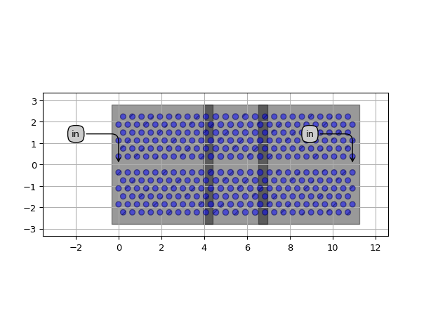
W1HeteroCavity1Mirror
- class picazzo3.phc.hetero.cell.W1HeteroCavity1Mirror
this partial component class forms a Cavity with a single mirror. It requires a second mirror to form a complete cavity
- Parameters:
- n_o_cladding_layers: int and number > 0
- cavity: PCell
The cavity child cell (autogenerated)
- mirror: PCell
The mirror child cell (autogenerated)
- cavity_defect_unit_cell: PCell
The Photonic Crystal unit cell of the cavity lattice. By default it is empty.
- mirror_defect_unit_cell: PCell
The Photonic Crystal unit cell of the mirror waveguide. By default it is empty.
- cavity_unit_cell: PCell
The Photonic Crystal unit cell of the cavity lattice
- mirror_unit_cell: PCell
The Photonic Crystal unit cell of the mirror lattice
- name: String that contains only ISO/IEC 8859-1 (extended ASCII py3) or pure ASCII (py2) characters
The unique name of the pcell
Views
- class Layout
- Parameters:
- cavity_pos: Coord2
- mirror_pos: Coord2
- purpose_hfw: PatternPurpose
- process_hfw: ProcessLayer
- vertical_cavity_pitch: float and number > 0
off-axis pitch of the cavity lattice: default = matched to mirror)
- vertical_mirror_pitch: float and number > 0
off-axis pitch of the mirror lattice: default = same as mirror_pitch)
- cavity_pitch: float and number > 0
- mirror_pitch: float and number > 0
- n_o_cavity_periods: int and number > 0
- n_o_mirror_periods: int and number > 0
- view_name: String that contains only alphanumeric characters from the ASCII set or contains _$. ASCII set is extended on PY3.
The name of the view
W1HeteroCavityMulti
- class picazzo3.phc.hetero.cell.W1HeteroCavityMulti
Photonic Crystal W1 Waveguide with multiple HeteroCavities with adjusted pitch in the cavity. The unit cells for the waveguide and the cavity can be chosen separately, as well as the different lattice pitches.
- Parameters:
- n_o_cladding_layers: int and number > 0
- cavity: PCell
The cavity child cell (autogenerated)
- mirror: PCell
The mirror child cell (autogenerated)
- cavity_defect_unit_cell: PCell
The Photonic Crystal unit cell of the cavity lattice. By default it is empty.
- mirror_defect_unit_cell: PCell
The Photonic Crystal unit cell of the mirror waveguide. By default it is empty.
- cavity_unit_cell: PCell
The Photonic Crystal unit cell of the cavity lattice
- mirror_unit_cell: PCell
The Photonic Crystal unit cell of the mirror lattice
- name: String that contains only ISO/IEC 8859-1 (extended ASCII py3) or pure ASCII (py2) characters
The unique name of the pcell
Views
- class Layout
- Parameters:
- cavity_period: float and number > 0
repetition period of the cavity. By default it is calculated automatically.
- n_o_cavities: int and number > 0
number of cavities in series
- mirror_pos2:
- cavity_pos: Coord2
- mirror_pos: Coord2
- purpose_hfw: PatternPurpose
- process_hfw: ProcessLayer
- vertical_cavity_pitch: float and number > 0
off-axis pitch of the cavity lattice: default = matched to mirror)
- vertical_mirror_pitch: float and number > 0
off-axis pitch of the mirror lattice: default = same as mirror_pitch)
- cavity_pitch: float and number > 0
- mirror_pitch: float and number > 0
- n_o_cavity_periods: int and number > 0
- n_o_mirror_periods: int and number > 0
- view_name: String that contains only alphanumeric characters from the ASCII set or contains _$. ASCII set is extended on PY3.
The name of the view
Examples
import si_fab.all as pdk  # noqa: F401
from picazzo3.phc.generic import DodecHole

mirror_unit_cell = DodecHole(name="Hc1")
mirror_unit_cell.Layout(radius=0.13)
cavity_unit_cell = DodecHole(name="Hc2")
cavity_unit_cell.Layout(radius=0.14)

# If we combine two hetero-interfaces, we get a Cavity.
from picazzo3.phc.hetero import W1HeteroCavityMulti

cell = W1HeteroCavityMulti(
    name="my_multihetero_cavity", mirror_unit_cell=mirror_unit_cell, cavity_unit_cell=cavity_unit_cell
)
layout = cell.Layout(
    n_o_cladding_layers=6,
    mirror_pitch=0.43,
    cavity_pitch=0.46,
    n_o_mirror_periods=10,
    n_o_cavity_periods=6,
    n_o_cavities=3,
)

layout.visualize(annotate=True)
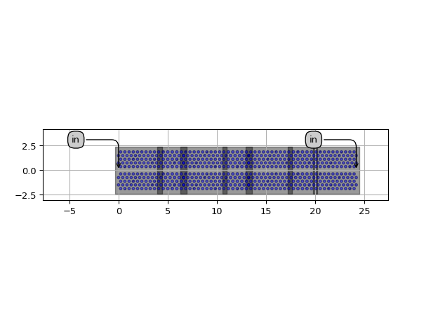
Photonic Crystal W1 Waveguides and Cavities
GenericW1Waveguide
- class picazzo3.phc.w1.cell.GenericW1Waveguide
A generic W1 Photonic Crystal waveguide. The unit cells can be specified as PCells, going outward as from the center line.
- Parameters:
- unit_cells: List with type restriction, allowed types: <class ‘ipkiss3.pcell.cell.pcell.PCell’>
List of unit cells: center row to outside rows (symmetric)
- name: String that contains only ISO/IEC 8859-1 (extended ASCII py3) or pure ASCII (py2) characters
The unique name of the pcell
Views
- class Layout
- Parameters:
- n_o_periods: int and number > 0
number of lattice periods in the propagation direction of the W1 waveguide
- start_even: ( bool, bool_ or int )
If true, start the crystal on an even row, if false, on an odd row.
- port_offset: float
Horizontal offset of the port width respect to the first and last column of the W1 waveguide.
- port_width: ( float and number > 0 ), *None allowed*
width of the waveguide ports of the photonic crystal waveguide. If none, a width of sqrt(3)*pitch is taken.
- port_row: ( int and number >= 0 ), *None allowed*
Row of the photonic crystal waveguide where the input/output ports are located. If none, it will be the center.
- pitch: float and Real, number and number >= 0
Lattice constant for a uniform triangular lattice. This property will be ignored if ‘lattice_pitches’ or ‘pitches’ are set manually
- lattice_pitches: Coord2 and number >= 0
Lattice constants along the horizontal and the oblique direction. Choose identical values for a regular grid. If ‘pitches’ is manually set, this property will be ignored. If this property is set, the property ‘pitch’ will be ignored.
- ports_coordinates:
list of tuple with (coordinate (in pitches), angle, waveguide_template, [name])
- zero_line_y: float
line in the map which corresponds to the coordinate y=0. This can be a fractional number, and the unit is relative to pitches.y .
- purpose_hfw: PatternPurpose
drawing purpose for underetching
- process_hfw: ProcessLayer
process for underetching
- map: str and String that contains only ISO/IEC 8859-1 (extended ASCII py3) or pure ASCII (py2) characters
Map of the photonic crystal. This property accepts a multi-line string. Every character in the string represents a unit cell of the photonic crystal, which can be found in the property cells
- cells: dict
dictionary of Unit Cells for a Photonic Crystal. The value should be of the form {‘x’: cell1, ‘y’: cell2}. The keys of the dictionary should be characters and each character can be used to identify the unit cell in the map
- pitches:
Cartesian (X, Y) pitches of the lattice. If this is specified, the properties ‘lattice_pitches’ and ‘pitch’ will be ignored
- view_name: String that contains only alphanumeric characters from the ASCII set or contains _$. ASCII set is extended on PY3.
The name of the view
Examples
"""We will generate a W1 with a lattice pitch which is slightly
different along the horizontal and oblique direction
"""

import si_fab.all as pdk  # noqa: F401
from picazzo3.phc.generic import DodecHole
from picazzo3.phc.w1 import GenericW1Waveguide

radii = [0.11, 0.11, 0.12, 0.12]  # inner holes are smaller than outer holes
centers = [(0.10, 0), (0, 0), (0, 0), (0, 0)]  # the inner rows are slightly displaced
unit_cells = [DodecHole().Layout(center=c, radius=r, angle=0) for (r, c) in zip(radii, centers)]

print(unit_cells)
# add them together, with an empty cell in the center
unit_cells = unit_cells[::-1] + [None] + unit_cells

cell = GenericW1Waveguide(name="my_generic_phc_waveguide1", unit_cells=unit_cells)
layout = cell.Layout(
    unit_cells=unit_cells,
    lattice_pitches=(0.43, 0.45),
    n_o_periods=22,
)

layout.visualize(annotate=True)
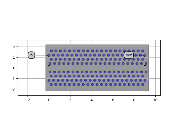
W1Waveguide
- class picazzo3.phc.w1.cell.W1Waveguide
A Uniform Photonic Crystal W1 waveguide consisting of 12-sided holes. You can specify the diameter of the lattice and the diameter of the defect holes in the core of the waveguide.
It is also possible to override the parameters of DodecPhCLayout, which allows you to customize the PCell in more detail.
- Parameters:
- name: String that contains only ISO/IEC 8859-1 (extended ASCII py3) or pure ASCII (py2) characters
The unique name of the pcell
Views
- class Layout
- Parameters:
- n_o_periods: int and number > 0
Number of lattice periods in the propagation direction.
- n_o_cladding_layers: int and number > 0
Number of cladding layers north and south.
- defect_diameter: float and Real, number and number >= 0
Diameter of the defect holes. If zero, no holes are drawn.
- diameter: float and number > 0
diameter of the photonic crystal lattice holes
- purpose: PatternPurpose
Purpose of the layer on which the holes should be drawn.
- process_wg: ProcessLayer
Process of the layer on which the holes should be drawn.
- hole_sizes: dict
dictionary of the hole sizes of the Photonic Crystal. The value should be of the form {‘x’: 0.25, ‘y’: 0.26}. The keys of the dictionary should be characters and each character can be used to identify the unit cell in the map. If the property ‘cells’ is set manually, hole_sizes’ will be ignored.
- pitch: float and Real, number and number >= 0
Lattice constant for a uniform triangular lattice. This property will be ignored if ‘lattice_pitches’ or ‘pitches’ are set manually
- lattice_pitches: Coord2 and number >= 0
Lattice constants along the horizontal and the oblique direction. Choose identical values for a regular grid. If ‘pitches’ is manually set, this property will be ignored. If this property is set, the property ‘pitch’ will be ignored.
- ports_coordinates:
list of tuple with (coordinate (in pitches), angle, waveguide_template, [name])
- zero_line_y: float
line in the map which corresponds to the coordinate y=0. This can be a fractional number, and the unit is relative to pitches.y .
- purpose_hfw: PatternPurpose
drawing purpose for underetching
- process_hfw: ProcessLayer
process for underetching
- map: str and String that contains only ISO/IEC 8859-1 (extended ASCII py3) or pure ASCII (py2) characters
Map of the photonic crystal. This property accepts a multi-line string. Every character in the string represents a unit cell of the photonic crystal, which can be found in the property cells
- cells:
dictionary of Unit Cells for a Photonic Crystal. The value should be of the form {‘x’: cell1, ‘y’: cell2}. The keys of the dictionary should be characters and each character can be used to identify the unit cell in the map. The default value of this property is automatically calculated from the dictionary ‘hole_sizes’. Only assign to this property if you want to override this value. If you do this, the property ‘hole_sizes’ will be ignored.
- pitches:
Cartesian (X, Y) pitches of the lattice. If this is specified, the properties ‘lattice_pitches’ and ‘pitch’ will be ignored
- view_name: String that contains only alphanumeric characters from the ASCII set or contains _$. ASCII set is extended on PY3.
The name of the view
Examples
"""A W1 waveguide with a missing row of holes"""
import si_fab.all as pdk  # noqa: F401
from picazzo3.phc.w1 import W1Waveguide

cell = W1Waveguide(name="my_w1")
layout = cell.Layout(
    pitch=0.43,  # lattice period of the triangular lattice
    diameter=0.28,  # hole diameter of the lattice
    n_o_cladding_layers=5,  # number of rows on each side of the defect
    n_o_periods=20,  # length of the lattice
)

layout.visualize(annotate=True)
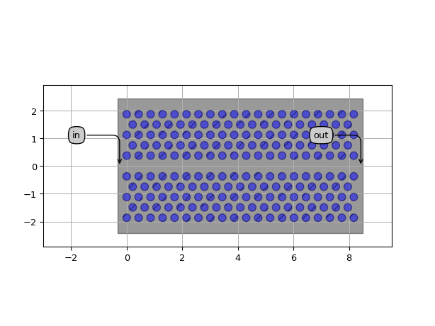
"""A W1 waveguide with a center row of holes of different size"""
import si_fab.all as pdk  # noqa: F401
from picazzo3.phc.w1 import W1Waveguide

cell = W1Waveguide(name="my_w1_with_defect")
layout = cell.Layout(
    pitch=0.43,  # lattice period of the triangular lattice
    diameter=0.28,  # hole diameter of the lattice
    defect_diameter=0.16,  # defect hole diameter
    n_o_cladding_layers=6,  # number of rows on each side of the defect
    n_o_periods=21,  # length of the lattice
)

layout.visualize(annotate=True)
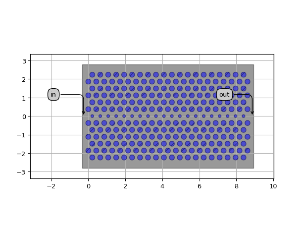
W1WaveguideWithInlineCavity
- class picazzo3.phc.w1.cell.W1WaveguideWithInlineCavity
A Uniform Photonic Crystal W1 waveguide with an inline cavity, consisting of 12-sided holes. You can specify the diameter of the lattice and the diameter of the defect holes in the core of the waveguide. The property ‘cavity_hole_diameters’ specifies the holes of the cavity from east to west.
It is also possible to override the parameters of DodecPhCLayout, which allows you to customize the PCell in more detail.
- Parameters:
- name: String that contains only ISO/IEC 8859-1 (extended ASCII py3) or pure ASCII (py2) characters
The unique name of the pcell
Views
- class Layout
- Parameters:
- cavity_hole_diameters: list<number >= 0>
list of hole diameters in the cavity, including mirrors
- n_o_periods: int and number > 0
Number of lattice periods in the propagation direction.
- n_o_cladding_layers: int and number > 0
Number of cladding layers north and south.
- defect_diameter: float and Real, number and number >= 0
Diameter of the defect holes. If zero, no holes are drawn.
- diameter: float and number > 0
diameter of the photonic crystal lattice holes
- purpose: PatternPurpose
Purpose of the layer on which the holes should be drawn.
- process_wg: ProcessLayer
Process of the layer on which the holes should be drawn.
- hole_sizes: dict
dictionary of the hole sizes of the Photonic Crystal. The value should be of the form {‘x’: 0.25, ‘y’: 0.26}. The keys of the dictionary should be characters and each character can be used to identify the unit cell in the map. If the property ‘cells’ is set manually, hole_sizes’ will be ignored.
- pitch: float and Real, number and number >= 0
Lattice constant for a uniform triangular lattice. This property will be ignored if ‘lattice_pitches’ or ‘pitches’ are set manually
- lattice_pitches: Coord2 and number >= 0
Lattice constants along the horizontal and the oblique direction. Choose identical values for a regular grid. If ‘pitches’ is manually set, this property will be ignored. If this property is set, the property ‘pitch’ will be ignored.
- ports_coordinates:
list of tuple with (coordinate (in pitches), angle, waveguide_template, [name])
- zero_line_y: float
line in the map which corresponds to the coordinate y=0. This can be a fractional number, and the unit is relative to pitches.y .
- purpose_hfw: PatternPurpose
drawing purpose for underetching
- process_hfw: ProcessLayer
process for underetching
- map: str and String that contains only ISO/IEC 8859-1 (extended ASCII py3) or pure ASCII (py2) characters
Map of the photonic crystal. This property accepts a multi-line string. Every character in the string represents a unit cell of the photonic crystal, which can be found in the property cells
- cells:
dictionary of Unit Cells for a Photonic Crystal. The value should be of the form {‘x’: cell1, ‘y’: cell2}. The keys of the dictionary should be characters and each character can be used to identify the unit cell in the map. The default value of this property is automatically calculated from the dictionary ‘hole_sizes’. Only assign to this property if you want to override this value. If you do this, the property ‘hole_sizes’ will be ignored.
- pitches:
Cartesian (X, Y) pitches of the lattice. If this is specified, the properties ‘lattice_pitches’ and ‘pitch’ will be ignored
- view_name: String that contains only alphanumeric characters from the ASCII set or contains _$. ASCII set is extended on PY3.
The name of the view
Examples
import si_fab.all as pdk  # noqa: F401
from picazzo3.phc.w1 import W1WaveguideWithInlineCavity

cell = W1WaveguideWithInlineCavity(name="my_w1_with_cavity")
layout = cell.Layout(
    pitch=0.43,  # lattice period of the triangular lattice
    diameter=0.28,  # hole diameter of the lattice
    n_o_cladding_layers=5,  # number of rows on each side of the defect
    n_o_periods=20,  # length of the lattice
    cavity_hole_diameters=[0.14, 0.16, 0.18, 0.21, 0.0, 0.21, 0.18, 0.16, 0.14],
)

layout.visualize(annotate=True)
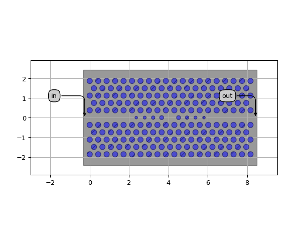
W1WaveguideWithAllpass
- class picazzo3.phc.w1.cell.W1WaveguideWithAllpass
A Uniform Photonic Crystal W1 waveguide with a lateral cavity (e.g. L3), consisting of 12-sided holes. You can specify the diameter of the lattice and the diameter of the defect holes in the core of the waveguide. The property ‘cavity_hole_diameters’ specifies the holes of the cavity from east to west.
- Parameters:
- name: String that contains only ISO/IEC 8859-1 (extended ASCII py3) or pure ASCII (py2) characters
The unique name of the pcell
Views
- class Layout
- Parameters:
- cavity_offset: int and number > 0
side row on which the cavity should be located
- cavity_length: int and number > 0
number of holes the cavity should be long
- n_o_periods: int and number > 0
Number of lattice periods in the propagation direction.
- n_o_cladding_layers: int and number > 0
Number of cladding layers north and south.
- defect_diameter: float and Real, number and number >= 0
Diameter of the defect holes. If zero, no holes are drawn.
- diameter: float and number > 0
diameter of the photonic crystal lattice holes
- purpose: PatternPurpose
Purpose of the layer on which the holes should be drawn.
- process_wg: ProcessLayer
Process of the layer on which the holes should be drawn.
- hole_sizes: dict
dictionary of the hole sizes of the Photonic Crystal. The value should be of the form {‘x’: 0.25, ‘y’: 0.26}. The keys of the dictionary should be characters and each character can be used to identify the unit cell in the map. If the property ‘cells’ is set manually, hole_sizes’ will be ignored.
- pitch: float and Real, number and number >= 0
Lattice constant for a uniform triangular lattice. This property will be ignored if ‘lattice_pitches’ or ‘pitches’ are set manually
- lattice_pitches: Coord2 and number >= 0
Lattice constants along the horizontal and the oblique direction. Choose identical values for a regular grid. If ‘pitches’ is manually set, this property will be ignored. If this property is set, the property ‘pitch’ will be ignored.
- ports_coordinates:
list of tuple with (coordinate (in pitches), angle, waveguide_template, [name])
- zero_line_y: float
line in the map which corresponds to the coordinate y=0. This can be a fractional number, and the unit is relative to pitches.y .
- purpose_hfw: PatternPurpose
drawing purpose for underetching
- process_hfw: ProcessLayer
process for underetching
- map: str and String that contains only ISO/IEC 8859-1 (extended ASCII py3) or pure ASCII (py2) characters
Map of the photonic crystal. This property accepts a multi-line string. Every character in the string represents a unit cell of the photonic crystal, which can be found in the property cells
- cells:
dictionary of Unit Cells for a Photonic Crystal. The value should be of the form {‘x’: cell1, ‘y’: cell2}. The keys of the dictionary should be characters and each character can be used to identify the unit cell in the map. The default value of this property is automatically calculated from the dictionary ‘hole_sizes’. Only assign to this property if you want to override this value. If you do this, the property ‘hole_sizes’ will be ignored.
- pitches:
Cartesian (X, Y) pitches of the lattice. If this is specified, the properties ‘lattice_pitches’ and ‘pitch’ will be ignored
- view_name: String that contains only alphanumeric characters from the ASCII set or contains _$. ASCII set is extended on PY3.
The name of the view
Examples
import si_fab.all as pdk  # noqa: F401
from picazzo3.phc.w1 import W1WaveguideWithAllpass

cell = W1WaveguideWithAllpass(name="my_w1_with_L_cavity")
layout = cell.Layout(
    pitch=0.43,  # lattice period of the triangular lattice
    diameter=0.28,  # hole diameter of the lattice
    n_o_cladding_layers=5,  # number of rows on each side of the defect
    n_o_periods=20,  # length of the lattice
    cavity_length=2,  # number of holes in the cavity
    cavity_offset=4,  # line from the center of the cavity
)

layout.visualize(annotate=True)
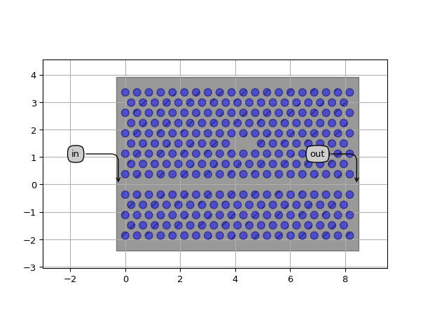
Traces
Rib Waveguides
RibWaveguideTemplate
- class picazzo3.traces.rib_wg.RibWaveguideTemplate
This waveguide is a (shallow etched) rib waveguide, with no specific bound in the slab.
                 core_width
               <----------->
               cladding_width
<------------------------------------------>
                ___________
_______________|           |________________

____________________________________________
- Parameters:
- name: String that contains only ISO/IEC 8859-1 (extended ASCII py3) or pure ASCII (py2) characters
The unique name of the pcell
Views
- class Layout
- Parameters:
- cladding_width: float and number > 0
total width of the waveguide with cladding
- cladding_purpose: PatternPurpose
drawing purpose layer for the cladding
- cladding_process: ProcessLayer
process for the waveguide cladding, defaults to the core process
- core_purpose: PatternPurpose
drawing purpose for the waveguide core
- core_process: ProcessLayer
process of the rib
- windows: List with type restriction, allowed types: <class ‘ipkiss3.pcell.trace.window.window._TraceWindow’>
List of Trace Windows that know how to draw themselves relative to the shape of the Trace
- core_width: float and number > 0
width of the rib
- core_layer: __Layer__
layer used to define the core of the waveguide
- pin_shape: Shape
shape to be used for the pins
- trace_template_for_ports: _TraceTemplate.Layout
Trace template to be used for the ports. Default = this template
- width: float and Real, number and number >= 0
- control_shape_layer: __Layer__
layer on which the control shape is drawn
- draw_control_shape: ( bool, bool_ or int )
draws the control shape on top of the waveguide
- cover_layers: List with type restriction, allowed types: <class ‘ipkiss.primitives.layer.Layer’>
layers that can be used to generate additional coverage of the trace (e.g. manhattan corners)
- view_name: String that contains only alphanumeric characters from the ASCII set or contains _$. ASCII set is extended on PY3.
The name of the view
Examples
"""This example shows how you use the template to directly create a rib waveguide PCell
and its layout."""
import si_fab.all as pdk  # noqa: F401
from ipkiss3 import all as i3
from picazzo3.traces.rib_wg.trace import RibWaveguideTemplate

wg_t = RibWaveguideTemplate(name="my_rib_wg_template1")
wg_t.Layout(core_width=0.47, cladding_width=2 * 3.0 + 0.47, core_process=i3.TECH.PROCESS.RWG)

wg = wg_t(name="my_rib_waveguide1")
layout = wg.Layout(shape=[(0.0, 0.0), (10.0, 0.0)])

layout.visualize(annotate=True)
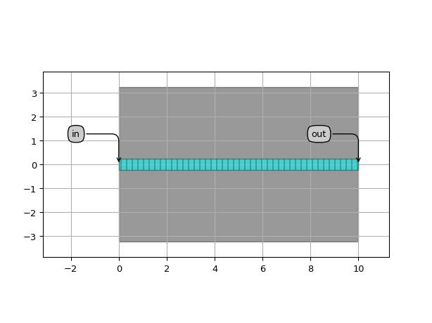
RibWireWaveguideTemplate
- class picazzo3.traces.rib_wg.RibWireWaveguideTemplate
This waveguide is a (shallow etched) rib waveguide, loaded on top of a (finite) strip wire.
                 core_width
               <----------->
                 strip_width
          <--------------------->
               cladding_width
<------------------------------------------>
                ___________
           ____|           |____
          |                     |
__________|_____________________|___________
- Parameters:
- name: String that contains only ISO/IEC 8859-1 (extended ASCII py3) or pure ASCII (py2) characters
The unique name of the pcell
Views
- class Layout
- Parameters:
- strip_cladding_purpose: PatternPurpose
drawing purpose for the strip wire cladding
- strip_purpose: PatternPurpose
drawing purpose for the strip wire
- strip_process: ProcessLayer
process for the strip wire
- strip_width: float and number > 0
width of the deep-etched strip wire
- cladding_width: float and number > 0
total width of the waveguide with cladding
- cladding_purpose: PatternPurpose
drawing purpose layer for the cladding
- cladding_process: ProcessLayer
process for the waveguide cladding, defaults to the core process
- core_purpose: PatternPurpose
drawing purpose for the waveguide core
- core_process: ProcessLayer
process for the shallow-etched core
- windows: List with type restriction, allowed types: <class ‘ipkiss3.pcell.trace.window.window._TraceWindow’>
List of Trace Windows that know how to draw themselves relative to the shape of the Trace
- core_width: float and number > 0
width of the shallow-etched core
- core_layer: __Layer__
layer used to define the core of the waveguide
- pin_shape: Shape
shape to be used for the pins
- trace_template_for_ports: _TraceTemplate.Layout
Trace template to be used for the ports. Default = this template
- width: float and Real, number and number >= 0
- control_shape_layer: __Layer__
layer on which the control shape is drawn
- draw_control_shape: ( bool, bool_ or int )
draws the control shape on top of the waveguide
- cover_layers: List with type restriction, allowed types: <class ‘ipkiss.primitives.layer.Layer’>
layers that can be used to generate additional coverage of the trace (e.g. manhattan corners)
- view_name: String that contains only alphanumeric characters from the ASCII set or contains _$. ASCII set is extended on PY3.
The name of the view
Examples
"""This example shows how you use the template to directly create a rib-wire waveguide PCell
and its layout."""
import si_fab.all as pdk  # noqa: F401
from ipkiss3 import all as i3
from picazzo3.traces.rib_wg.trace import RibWireWaveguideTemplate

wg_t = RibWireWaveguideTemplate(name="my_ribwire_wg_template1")
wg_t.Layout(
    core_width=0.4,
    strip_width=1.2,
    cladding_width=2 * 4.0 + 1.2,
    core_process=i3.TECH.PROCESS.RWG,
    strip_process=i3.TECH.PROCESS.WG,
)

wg = wg_t(name="my_ribwire_waveguide1")
layout = wg.Layout(shape=[(0.0, 0.0), (10.0, 0.0)])

layout.visualize(annotate=True)
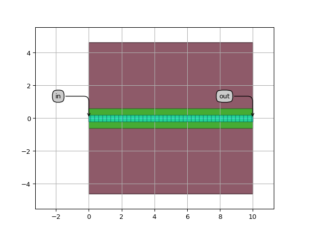
Slot Waveguides
SlotWaveguideTemplate
- class picazzo3.traces.slot_wg.SlotWaveguideTemplate
This waveguide is a strip-like waveguide with a slot in the middle.
                ____   ____
               |    | |    |
               |    | |    |
_______________|____|_|____|_________________
The core width is defined as the total width covering both slots. (i.e., slot_width should be < core_width).
- Parameters:
- name: String that contains only ISO/IEC 8859-1 (extended ASCII py3) or pure ASCII (py2) characters
The unique name of the pcell
Views
- class Layout
- Parameters:
- slot_purpose: PatternPurpose
drawing purpose for the slot
- slot_process: ProcessLayer
process for the slot
- slot_width: float and number > 0
width of the slot
- cladding_width: float and number > 0
total width of the waveguide with cladding
- cladding_purpose: PatternPurpose
drawing purpose layer for the cladding
- cladding_process: ProcessLayer
process for the waveguide cladding, defaults to the core process
- core_purpose: PatternPurpose
drawing purpose for the waveguide ribs
- core_process: ProcessLayer
process for the waveguide ribs
- windows: List with type restriction, allowed types: <class ‘ipkiss3.pcell.trace.window.window._TraceWindow’>
List of Trace Windows that know how to draw themselves relative to the shape of the Trace
- core_width: float and number > 0
width of the waveguide core
- core_layer: __Layer__
layer used to define the core of the waveguide
- pin_shape: Shape
shape to be used for the pins
- trace_template_for_ports: _TraceTemplate.Layout
Trace template to be used for the ports. Default = this template
- width: float and Real, number and number >= 0
- control_shape_layer: __Layer__
layer on which the control shape is drawn
- draw_control_shape: ( bool, bool_ or int )
draws the control shape on top of the waveguide
- cover_layers: List with type restriction, allowed types: <class ‘ipkiss.primitives.layer.Layer’>
layers that can be used to generate additional coverage of the trace (e.g. manhattan corners)
- view_name: String that contains only alphanumeric characters from the ASCII set or contains _$. ASCII set is extended on PY3.
The name of the view
Examples
"""This example shows how you use the template to directly create a slot waveguide PCell
and its layout."""
import si_fab.all as pdk  # noqa: F401
import ipkiss3.all as i3
from picazzo3.traces.slot_wg.trace import SlotWaveguideTemplate

wg_t = SlotWaveguideTemplate(name="my_slot_wg_template1")
wg_t.Layout(
    core_width=0.5, slot_width=0.12, cladding_width=2 * 3.0 + 0.5, slot_purpose=i3.TECH.PURPOSE.DRWSUB
)

wg = wg_t(name="my_slot_waveguide1")
layout = wg.Layout(shape=[(0.0, 0.0), (10.0, 0.0)])

layout.visualize(annotate=True)
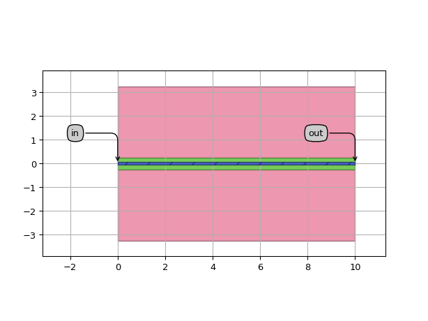
DoubleSlotWaveguideTemplate
- class picazzo3.traces.slot_wg.DoubleSlotWaveguideTemplate
This waveguide is a strip-like waveguide with two slots in the middle
                ___   __   ___
               |   | |  | |   |
               |   | |  | |   |
_______________|___|_|  |_|___|_________________
- Parameters:
- name: String that contains only ISO/IEC 8859-1 (extended ASCII py3) or pure ASCII (py2) characters
The unique name of the pcell
Views
- class Layout
- Parameters:
- center_core_width: float and number > 0
- slot_purpose: PatternPurpose
drawing purpose for the slot
- slot_process: ProcessLayer
process for the slot
- slot_width: float and number > 0
width of the slot
- cladding_width: float and number > 0
total width of the waveguide with cladding
- cladding_purpose: PatternPurpose
drawing purpose layer for the cladding
- cladding_process: ProcessLayer
process for the waveguide cladding, defaults to the core process
- core_purpose: PatternPurpose
drawing purpose for the waveguide ribs
- core_process: ProcessLayer
process for the waveguide ribs
- windows: List with type restriction, allowed types: <class ‘ipkiss3.pcell.trace.window.window._TraceWindow’>
List of Trace Windows that know how to draw themselves relative to the shape of the Trace
- core_width: float and number > 0
- core_layer: __Layer__
layer used to define the core of the waveguide
- pin_shape: Shape
shape to be used for the pins
- trace_template_for_ports: _TraceTemplate.Layout
Trace template to be used for the ports. Default = this template
- width: float and Real, number and number >= 0
- control_shape_layer: __Layer__
layer on which the control shape is drawn
- draw_control_shape: ( bool, bool_ or int )
draws the control shape on top of the waveguide
- cover_layers: List with type restriction, allowed types: <class ‘ipkiss.primitives.layer.Layer’>
layers that can be used to generate additional coverage of the trace (e.g. manhattan corners)
- view_name: String that contains only alphanumeric characters from the ASCII set or contains _$. ASCII set is extended on PY3.
The name of the view
Examples
"""This example shows how you use the template to directly create a slot waveguide PCell
and its layout."""
import si_fab.all as pdk  # noqa: F401
from picazzo3.traces.slot_wg.trace import DoubleSlotWaveguideTemplate

wg_t = DoubleSlotWaveguideTemplate(name="my_doubleslot_wg_template1")
wg_t.Layout(core_width=0.6, slot_width=0.12, center_core_width=0.12, cladding_width=2 * 3.0 + 0.6)

wg = wg_t(name="my_doubleslot_waveguide1")
layout = wg.Layout(shape=[(0.0, 0.0), (10.0, 0.0)])

layout.visualize(annotate=True)

Socket Waveguides
SocketWaveguideTemplate
- class picazzo3.traces.socket_wg.SocketWaveguideTemplate
Socket-style waveguide template: deep etched rib waveguide
                ___________
               |           |
_______________|           |________________
____________________________________________
- Parameters:
- name: String that contains only ISO/IEC 8859-1 (extended ASCII py3) or pure ASCII (py2) characters
The unique name of the pcell
Views
- class Layout
- Parameters:
- cladding_width: float and number > 0
total width of the waveguide with cladding
- cladding_purpose: PatternPurpose
drawing purpose layer for the cladding
- cladding_process: ProcessLayer
process for the waveguide cladding, defaults to the core process
- core_purpose: PatternPurpose
drawing purpose for the waveguide core
- core_process: ProcessLayer
process for the rib
- windows: List with type restriction, allowed types: <class ‘ipkiss3.pcell.trace.window.window._TraceWindow’>
List of Trace Windows that know how to draw themselves relative to the shape of the Trace
- core_width: float and number > 0
width of the rib
- core_layer: __Layer__
layer used to define the core of the waveguide
- pin_shape: Shape
shape to be used for the pins
- trace_template_for_ports: _TraceTemplate.Layout
Trace template to be used for the ports. Default = this template
- width: float and Real, number and number >= 0
- control_shape_layer: __Layer__
layer on which the control shape is drawn
- draw_control_shape: ( bool, bool_ or int )
draws the control shape on top of the waveguide
- cover_layers: List with type restriction, allowed types: <class ‘ipkiss.primitives.layer.Layer’>
layers that can be used to generate additional coverage of the trace (e.g. manhattan corners)
- view_name: String that contains only alphanumeric characters from the ASCII set or contains _$. ASCII set is extended on PY3.
The name of the view
Examples
"""This example shows how you use the template to directly create a socket waveguide PCell
and its layout."""
import si_fab.all as pdk  # noqa: F401
from picazzo3.traces.socket_wg.trace import SocketWaveguideTemplate

wg_t = SocketWaveguideTemplate(name="my_socket_wg_template1")
wg_t.Layout(core_width=0.5, cladding_width=2 * 3.0 + 0.5)

wg = wg_t(name="my_socket_waveguide1")
layout = wg.Layout(shape=[(0.0, 0.0), (10.0, 0.0)])

layout.visualize(annotate=True)
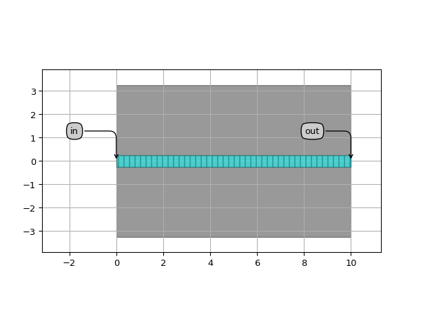
SlottedSocketWaveguideTemplate
- class picazzo3.traces.socket_wg.SlottedSocketWaveguideTemplate
Socket waveguide with a deep etched slot
                ____   ____
               |    | |    |
_______________|    | |    |________________
____________________|_|_____________________
- Parameters:
- name: String that contains only ISO/IEC 8859-1 (extended ASCII py3) or pure ASCII (py2) characters
The unique name of the pcell
Views
- class Layout
- Parameters:
- slot_purpose: PatternPurpose
drawing purpose for the slot
- slot_process: ProcessLayer
process for the slot
- slot_width: float and number > 0
width of the slot
- cladding_width: float and number > 0
total width of the waveguide with cladding
- cladding_purpose: PatternPurpose
drawing purpose layer for the cladding
- cladding_process: ProcessLayer
process for the waveguide cladding, defaults to the core process
- core_purpose: PatternPurpose
drawing purpose for the waveguide ribs
- core_process: ProcessLayer
process for the rib
- windows: List with type restriction, allowed types: <class ‘ipkiss3.pcell.trace.window.window._TraceWindow’>
List of Trace Windows that know how to draw themselves relative to the shape of the Trace
- core_width: float and number > 0
width of the waveguide core
- core_layer: __Layer__
layer used to define the core of the waveguide
- pin_shape: Shape
shape to be used for the pins
- trace_template_for_ports: _TraceTemplate.Layout
Trace template to be used for the ports. Default = this template
- width: float and Real, number and number >= 0
- control_shape_layer: __Layer__
layer on which the control shape is drawn
- draw_control_shape: ( bool, bool_ or int )
draws the control shape on top of the waveguide
- cover_layers: List with type restriction, allowed types: <class ‘ipkiss.primitives.layer.Layer’>
layers that can be used to generate additional coverage of the trace (e.g. manhattan corners)
- view_name: String that contains only alphanumeric characters from the ASCII set or contains _$. ASCII set is extended on PY3.
The name of the view
Examples
"""This example shows how you use the template to directly create a slotted socket waveguide PCell
and its layout."""
import si_fab.all as pdk  # noqa: F401
from picazzo3.traces.socket_wg.trace import SlottedSocketWaveguideTemplate

wg_t = SlottedSocketWaveguideTemplate(name="my_slottedsocket_wg_template1")
wg_t.Layout(core_width=0.5, slot_width=0.15, cladding_width=2 * 3.0 + 0.5)

wg = wg_t(name="my_slottedsocket_waveguide1")
layout = wg.Layout(shape=[(0.0, 0.0), (10.0, 0.0)])

layout.visualize(annotate=True)
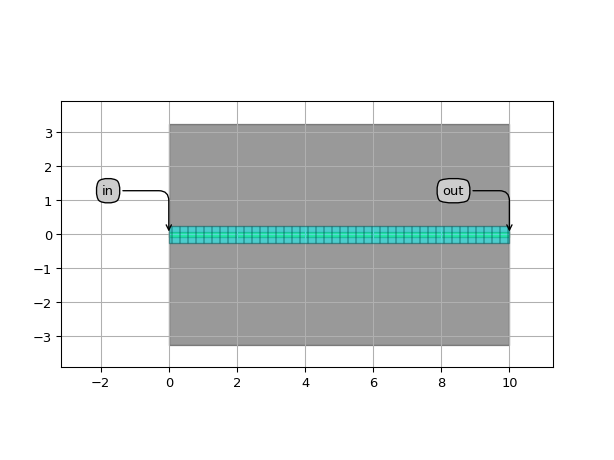
Thinned Waveguides
ThinnedWaveguideTemplate
- class picazzo3.traces.thin_wg.ThinnedWaveguideTemplate
Thinned waveguide.
Takes an existing waveguide template (given by trace_template) and overlay with a thinning layer.
- Parameters:
- trace_template: PCell and _TraceTemplate
Refers to the other trace template from which information is taken to build this trace template.
- name: String that contains only ISO/IEC 8859-1 (extended ASCII py3) or pure ASCII (py2) characters
The unique name of the pcell
Views
- class Layout
- Parameters:
- thin_width: float and Real, number and number >= 0
width of the thinning layer
- thin_purpose: PatternPurpose
drawing purpose for the thinning region
- thin_process: ProcessLayer
thinning process
- cladding_process: ProcessLayer
process for the waveguide cladding, defaults to the core process
- core_purpose: PatternPurpose
drawing purpose for the waveguide core
- core_process: ProcessLayer
process for the waveguide core
- cladding_width: float and number > 0
total width of the waveguide with cladding
- cladding_purpose: PatternPurpose
drawing purpose layer for the cladding
- core_width: float and number > 0
width of the waveguide core
- core_layer: __Layer__
layer used to define the core of the waveguide
- flatten_contents: ( bool, bool_ or int )
if True, it will insert the referred trace as elements in the layout, rather than as an Instance
- pin_shape: Shape
shape to be used for the pins
- trace_template_for_ports: _TraceTemplate.Layout
Trace template to be used for the ports. Default = this template
- windows: List with type restriction, allowed types: <class ‘ipkiss3.pcell.trace.window.window._TraceWindow’>
List of Trace Windows that know how to draw themselves relative to the shape of the Trace
- keep_original_trace_template: ( bool, bool_ or int )
- width: float and Real, number and number >= 0
- control_shape_layer: __Layer__
layer on which the control shape is drawn
- draw_control_shape: ( bool, bool_ or int )
draws the control shape on top of the waveguide
- cover_layers: List with type restriction, allowed types: <class ‘ipkiss.primitives.layer.Layer’>
layers that can be used to generate additional coverage of the trace (e.g. manhattan corners)
- view_name: String that contains only alphanumeric characters from the ASCII set or contains _$. ASCII set is extended on PY3.
The name of the view
Examples
"""This example shows how you use the template to directly create a thinned waveguide PCell
and its layout.
"""
import si_fab.all as pdk  # noqa: F401
from ipkiss3 import all as i3
from picazzo3.traces.wire_wg.trace import WireWaveguideTemplate
from picazzo3.traces.thin_wg.trace import ThinnedWaveguideTemplate

wg_t = WireWaveguideTemplate(name="my_wire_wg_template1")
wg_t.Layout(core_width=0.47, cladding_width=2 * 3.0 + 0.47, core_process=i3.TECH.PROCESS.WG)

thinwg_t = ThinnedWaveguideTemplate(trace_template=wg_t, name="my_thin_wg_template1")
thinwg_t.Layout(thin_process=i3.TECH.PROCESS.FC, thin_width=1.2)

wg = thinwg_t(name="my_thin_waveguide1")
layout = wg.Layout(shape=[(0.0, 0.0), (10.0, 0.0)])

layout.visualize(annotate=True)
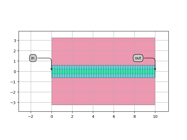
Wire Waveguides
WireWaveguideTemplate
- class picazzo3.traces.wire_wg.WireWaveguideTemplate
Wire-like waveguide definition, with a core and a cladding. The waveguide is defined as a ‘cladding area’ (i.e. a cladding zone where the trench will be etched or other material will be), and a ‘core area’, which draws the shape of the waveguide core inside the ‘cladding area’.
The waveguide can be drawn on different processes, by default it is the WG process.
          core_width
          <-------->
        cladding_width
<------------------------------>
           ________
          |        |
__________|        |____________
- Parameters:
- name: String that contains only ISO/IEC 8859-1 (extended ASCII py3) or pure ASCII (py2) characters
The unique name of the pcell
Views
- class Layout
- Parameters:
- cladding_width: float and number > 0
total width of the waveguide with cladding
- cladding_purpose: PatternPurpose
drawing purpose layer for the cladding
- cladding_process: ProcessLayer
process for the waveguide cladding, defaults to the core process
- core_purpose: PatternPurpose
drawing purpose for the waveguide core
- core_process: ProcessLayer
process for the waveguide core
- windows: List with type restriction, allowed types: <class ‘ipkiss3.pcell.trace.window.window._TraceWindow’>
List of Trace Windows that know how to draw themselves relative to the shape of the Trace
- core_width: float and number > 0
width of the waveguide core
- core_layer: __Layer__
layer used to define the core of the waveguide
- pin_shape: Shape
shape to be used for the pins
- trace_template_for_ports: _TraceTemplate.Layout
Trace template to be used for the ports. Default = this template
- width: float and Real, number and number >= 0
- control_shape_layer: __Layer__
layer on which the control shape is drawn
- draw_control_shape: ( bool, bool_ or int )
draws the control shape on top of the waveguide
- cover_layers: List with type restriction, allowed types: <class ‘ipkiss.primitives.layer.Layer’>
layers that can be used to generate additional coverage of the trace (e.g. manhattan corners)
- view_name: String that contains only alphanumeric characters from the ASCII set or contains _$. ASCII set is extended on PY3.
The name of the view
Examples
"""This example shows how you use the template to directly create a waveguide PCell
and its layout."""
import si_fab.all as pdk  # noqa: F401
from ipkiss3 import all as i3
from picazzo3.traces.wire_wg.trace import WireWaveguideTemplate

wg_t = WireWaveguideTemplate(name="my_wire_wg_template1")
wg_t.Layout(core_width=0.47, cladding_width=2 * 3.0 + 0.47, core_process=i3.TECH.PROCESS.WG)

wg = wg_t(name="my_wire_waveguide1")
layout = wg.Layout(shape=[(0.0, 0.0), (10.0, 0.0), (15.0, 15.0)])

layout.visualize(annotate=True)
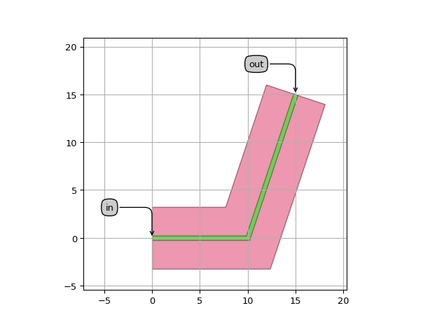
"""This example shows how you use the template as a parameter for a generic
Waveguide PCell."""
import si_fab.all as pdk  # noqa: F401
from ipkiss3 import all as i3
from picazzo3.traces.wire_wg.trace import WireWaveguideTemplate

wg_t = WireWaveguideTemplate(name="my_wire_wg_template2")
wg_t.Layout(core_width=0.47, cladding_width=2 * 3.0 + 0.47, core_process=i3.TECH.PROCESS.WG)

wg = i3.Waveguide(name="my_wire_waveguide2", trace_template=wg_t)
layout = wg.Layout(shape=[(0.0, 0.0), (10.0, 0.0), (15.0, 15.0)])

layout.visualize(annotate=True)

"""This example shows how you use the template as a parameter for a rounded
Waveguide PCell."""
import si_fab.all as pdk  # noqa: F401
from ipkiss3 import all as i3
from picazzo3.traces.wire_wg.trace import WireWaveguideTemplate

wg_t = WireWaveguideTemplate(name="my_wg_template3")
wg_t.Layout(core_width=0.47, cladding_width=2 * 3.0 + 0.47, core_process=i3.TECH.PROCESS.WG)

wg = i3.RoundedWaveguide(name="my_rounded_wire_waveguide1", trace_template=wg_t)
layout = wg.Layout(shape=[(0.0, 0.0), (10.0, 0.0), (15.0, 15.0)], bend_radius=7.0, manhattan=True)

layout.visualize(annotate=True)
Transitions
Rib Transitions
WireRibWaveguideTransitionLinear
- class picazzo3.traces.rib_wg.WireRibWaveguideTransitionLinear
Transition from/to wire (deep etched) to/from rib (shallow etched) waveguides.
You can provide either a wire for the start, and rib for the end, or vice versa. The wire_only_length is the part of the transition in which the rib part is gradually built up. After this length, we abruptly change to the rib waveguide. If the rib part is sufficiently wide in the first part, there should be no reflections at the interface.
- Parameters:
- modified_start_wg_template: PCell and _TraceTemplate
Modified start waveguide template (using the end_trace_template, but with the dimensions of the start_trace_template)
- wire_only_wg_template: PCell and _TraceTemplate
- end_trace_template: PCell and _TraceTemplate and WireWaveguideTemplate, RibWaveguideTemplate
- start_trace_template: PCell and _TraceTemplate and WireWaveguideTemplate, RibWaveguideTemplate
- name: String that contains only ISO/IEC 8859-1 (extended ASCII py3) or pure ASCII (py2) characters
The unique name of the pcell
- Other Parameters:
- reverse_templates: ( bool, bool_ or int ), locked
When True, treat start_trace_template as end_trace_template and vice versa. To use the correct templates, use the _{start/stop}_trace_template properties. This should not be set manually, but calculated by the transition itself.
Views
- class Layout
- Parameters:
- wire_only_cladding_width: float and number > 0
width of the cladding at the end of the wire_only_length
- wire_end_width: float and Real, number and number >= 0
width of the wire core at its end point.
- wire_only_length: ( float and Real, number and number >= 0 ), *None allowed*
Length of transition where shallow part is built up.
- straight_extension: Coord2 and number >= 0
tuple: straight extension at start and end of transition
- end_position: Coord2
end position of the transition
- start_position: Coord2
start position of the transition
- view_name: String that contains only alphanumeric characters from the ASCII set or contains _$. ASCII set is extended on PY3.
The name of the view
- Other Parameters:
- length: float and Real, number and number >= 0, locked
length of the transition
Examples
"""This example shows how you transition from a wire to a rib waveguide."""
import si_fab.all as pdk  # noqa: F401
import ipkiss3.all as i3

from picazzo3.traces.wire_wg import WireWaveguideTemplate
from picazzo3.traces.rib_wg import RibWaveguideTemplate
from picazzo3.traces.rib_wg import WireRibWaveguideTransitionLinear

wg_start = WireWaveguideTemplate()
wg_start.Layout(core_width=0.45, cladding_width=0.45 + 2 * i3.TECH.WG.TRENCH_WIDTH)
wg_end = RibWaveguideTemplate()
wg_end.Layout(core_width=0.9, cladding_width=0.9 + 2 * 3.0)

wg_deeponly = WireWaveguideTemplate()
wg_deeponly.Layout(core_width=3.0, cladding_width=3.0 + 2 * i3.TECH.WG.TRENCH_WIDTH)

t = WireRibWaveguideTransitionLinear(
    start_trace_template=wg_start, end_trace_template=wg_end, wire_only_wg_template=wg_deeponly
)

t_lay = t.Layout(
    start_position=(10.0, 0.0),
    end_position=(30.0, 0.0),
    wire_only_length=5.0,
    straight_extension=(0.3, 0.4),
)
t_lay.visualize(annotate=True)
WireRibWaveguideTransitionFromPortLinear
- class picazzo3.traces.rib_wg.WireRibWaveguideTransitionFromPortLinear
Transition from/to wire (deep etched) to/from rib (shallow etched) waveguides.
You can provide a start_port and end_trace_template.
- Parameters:
- wire_only_wg_template: PCell and _TraceTemplate
- modified_start_wg_template: PCell and _TraceTemplate
Modified start waveguide template (using the end_trace_template, but with the dimensions of the start_trace_template)
- start_port: _PortInterface
the port on which to extract trace template, position and angle
- end_trace_template: PCell and _TraceTemplate and WireWaveguideTemplate, RibWaveguideTemplate
- start_trace_template: PCell and _TraceTemplate and WireWaveguideTemplate, RibWaveguideTemplate
- name: String that contains only ISO/IEC 8859-1 (extended ASCII py3) or pure ASCII (py2) characters
The unique name of the pcell
- Other Parameters:
- reverse_templates: ( bool, bool_ or int ), locked
When True, treat start_trace_template as end_trace_template and vice versa. To use the correct templates, use the _{start/stop}_trace_template properties. This should not be set manually, but calculated by the transition itself.
Views
- class Layout
- Parameters:
- wire_only_length: ( float and Real, number and number >= 0 ), *None allowed*
Length of transition where shallow part is built up.
- wire_only_cladding_width: float and number > 0
width of the cladding at the end of the wire_only_length
- wire_end_width: float and Real, number and number >= 0
width of the wire core at its end point.
- straight_extension: Coord2 and number >= 0
tuple: straight extension at start and end of transition
- length: float and Real, number and number >= 0
length of the transition
- end_position: Coord2
end position of the transition
- start_position: Coord2
start position of the transition
- view_name: String that contains only alphanumeric characters from the ASCII set or contains _$. ASCII set is extended on PY3.
The name of the view
Examples
"""This example shows how to append a transition onto a component.
The component has a port, which is associated with a
WireWaveguideTemplate, and we want to taper to a RibWaveguideTemplate.
"""
import si_fab.all as pdk  # noqa: F401
from ipkiss3 import all as i3
from picazzo3.traces.wire_wg import WireWaveguideTemplate
from picazzo3.traces.rib_wg import RibWaveguideTemplate
from picazzo3.traces.rib_wg import WireRibWaveguideTransitionFromPortLinear

wg_start = WireWaveguideTemplate()
wg_start.Layout(core_width=0.45, cladding_width=0.45 + 2 * i3.TECH.WG.TRENCH_WIDTH)

wg_end = RibWaveguideTemplate()
wg_end.Layout(core_width=0.9, cladding_width=0.9 + 2 * i3.TECH.WG.TRENCH_WIDTH)

wg_wireonly = WireWaveguideTemplate()
wg_wireonly.Layout(core_width=3.0, cladding_width=3.0 + 2 * i3.TECH.WG.TRENCH_WIDTH)

class P(i3.PCell):
    out_trace_template = i3.TraceTemplateProperty()

    class Layout(i3.LayoutView):
        def _generate_ports(self, ports):
            return i3.OpticalPort(name="out", position=(3.0, 3.0), angle=10.0, trace_template=wg_start)

p = P(out_trace_template=wg_start)
p.Layout()

t = WireRibWaveguideTransitionFromPortLinear(
    start_port=(p, "out"), end_trace_template=wg_end, wire_only_wg_template=wg_wireonly
)

t_lay = t.Layout(length=15.0, straight_extension=(0.0, 0.2), wire_only_length=5.0)

t_lay.visualize(annotate=True)
Slot Transitions
SlottedWireWaveguideTransitionLinear
- class picazzo3.traces.slot_wg.SlottedWireWaveguideTransitionLinear
Transition from/to a slotted waveguide to/from a wire waveguide.
You can provide either a slotted waveguide for the start, and a wire waveguide for the end, or vica versa.
- Parameters:
- end_trace_template: PCell and _TraceTemplate and WireWaveguideTemplate, SlotWaveguideTemplate
- start_trace_template: PCell and _TraceTemplate and WireWaveguideTemplate, SlotWaveguideTemplate
- name: String that contains only ISO/IEC 8859-1 (extended ASCII py3) or pure ASCII (py2) characters
The unique name of the pcell
- Other Parameters:
- reverse_templates: ( bool, bool_ or int ), locked
When True, treat start_trace_template as end_trace_template and vice versa. To use the correct templates, use the _{start/stop}_trace_template properties. This should not be set manually, but calculated by the transition itself.
Views
- class Layout
- Parameters:
- tip_width: float and number > 0
- slot_extension_length: float and number > 0
- straight_extension: Coord2 and number >= 0
tuple: straight extension at start and end of transition
- end_position: Coord2
end position of the transition
- start_position: Coord2
start position of the transition
- view_name: String that contains only alphanumeric characters from the ASCII set or contains _$. ASCII set is extended on PY3.
The name of the view
- Other Parameters:
- length: float and Real, number and number >= 0, locked
length of the transition
Examples
"""This example shows how you transition from a wire to a slotted waveguide."""
import si_fab.all as pdk  # noqa: F401
from picazzo3.traces.wire_wg import WireWaveguideTemplate
from picazzo3.traces.slot_wg import SlotWaveguideTemplate, SlottedWireWaveguideTransitionLinear
from ipkiss3 import all as i3

wg_start_wire = WireWaveguideTemplate()
wg_start_wire.Layout(core_width=0.6, cladding_width=0.6 + 2 * i3.TECH.WG.TRENCH_WIDTH)

wg_start = SlotWaveguideTemplate()
wg_start.Layout(slot_width=0.15, cladding_width=1.0)

wg_end = WireWaveguideTemplate()
wg_end.Layout(core_width=0.6, cladding_width=0.6 + 2 * i3.TECH.WG.TRENCH_WIDTH)

t = SlottedWireWaveguideTransitionLinear(
    name="my_transition", start_trace_template=wg_start, end_trace_template=wg_end
)

t_lay = t.Layout(start_position=(3.0, 3.0), end_position=(23.0, 3.0), straight_extension=(0.3, 0.4))

t_lay.visualize(annotate=True)
SlottedWireWaveguideTransitionFromPortLinear
- class picazzo3.traces.slot_wg.SlottedWireWaveguideTransitionFromPortLinear
Linear transition from/to a slotted waveguide to/from a wire waveguide.
You can provide either a slotted waveguide for the start, and a wire waveguide for the end, or vica versa.
- Parameters:
- start_port: _PortInterface
the port on which to extract trace template, position and angle
- end_trace_template: PCell and _TraceTemplate and WireWaveguideTemplate, SlotWaveguideTemplate
- start_trace_template: PCell and _TraceTemplate and WireWaveguideTemplate, SlotWaveguideTemplate
- name: String that contains only ISO/IEC 8859-1 (extended ASCII py3) or pure ASCII (py2) characters
The unique name of the pcell
- Other Parameters:
- reverse_templates: ( bool, bool_ or int ), locked
When True, treat start_trace_template as end_trace_template and vice versa. To use the correct templates, use the _{start/stop}_trace_template properties. This should not be set manually, but calculated by the transition itself.
Views
- class Layout
- Parameters:
- slot_extension_length: float and number > 0
- tip_width: float and number > 0
- straight_extension: Coord2 and number >= 0
tuple: straight extension at start and end of transition
- length: float and Real, number and number >= 0
length of the transition
- end_position: Coord2
end position of the transition
- start_position: Coord2
start position of the transition
- view_name: String that contains only alphanumeric characters from the ASCII set or contains _$. ASCII set is extended on PY3.
The name of the view
Examples
"""This example shows how to append a transition onto a component.
The component has a port, which is associated with a
WireWaveguideTemplate, and we want to taper to a SlotWaveguideTemplate.
"""
import si_fab.all as pdk  # noqa: F401
from picazzo3.traces.wire_wg import WireWaveguideTemplate
from picazzo3.traces.slot_wg import SlotWaveguideTemplate, SlottedWireWaveguideTransitionFromPortLinear
from ipkiss3 import all as i3

wg_start = WireWaveguideTemplate()
wg_start.Layout(core_width=0.6, cladding_width=0.6 + 2 * i3.TECH.WG.TRENCH_WIDTH)

wg_end = SlotWaveguideTemplate()
wg_end.Layout(slot_width=0.15, cladding_width=1.0)

class P(i3.PCell):
    out_trace_template = i3.TraceTemplateProperty()

    class Layout(i3.LayoutView):
        def _generate_ports(self, ports):
            return i3.OpticalPort(name="out", position=(3.0, 3.0), angle=10.0, trace_template=wg_start)

p = P(out_trace_template=wg_start)
p.Layout()

t = SlottedWireWaveguideTransitionFromPortLinear(start_port=(p, "out"), end_trace_template=wg_end)

t_lay = t.Layout(length=15.0, straight_extension=(0.0, 0.2))

t_lay.visualize(annotate=True)
Socket Transitions
WireSocketWaveguideTransitionLinear
- class picazzo3.traces.socket_wg.WireSocketWaveguideTransitionLinear
Transition from/to wire (deep etched) to/from socket (deep etched rib) waveguides.
You can provide either a wire for the start, and socket for the end, or vice versa.
The wire_only_length is the part of the transition in which the socket part is gradually built up. After this length, we abruptly change to the socket waveguide. If the socket part is sufficiently wide in the first part, there should be no reflections at the interface.
- Parameters:
- modified_start_wg_template: PCell and _TraceTemplate
Modified start waveguide template (using the end_trace_template, but with the dimensions of the start_trace_template)
- wire_only_wg_template: PCell and _TraceTemplate
- end_trace_template: PCell and _TraceTemplate and WireWaveguideTemplate, SocketWaveguideTemplate
- start_trace_template: PCell and _TraceTemplate and WireWaveguideTemplate, SocketWaveguideTemplate
- name: String that contains only ISO/IEC 8859-1 (extended ASCII py3) or pure ASCII (py2) characters
The unique name of the pcell
- Other Parameters:
- reverse_templates: ( bool, bool_ or int ), locked
When True, treat start_trace_template as end_trace_template and vice versa. To use the correct templates, use the _{start/stop}_trace_template properties. This should not be set manually, but calculated by the transition itself.
Views
- class Layout
- Parameters:
- wire_only_cladding_width: float and number > 0
width of the cladding at the end of the wire_only_length
- wire_end_width: float and Real, number and number >= 0
width of the wire core at its end point.
- wire_only_length: ( float and Real, number and number >= 0 ), *None allowed*
Length of transition where shallow part is built up.
- straight_extension: Coord2 and number >= 0
tuple: straight extension at start and end of transition
- end_position: Coord2
end position of the transition
- start_position: Coord2
start position of the transition
- view_name: String that contains only alphanumeric characters from the ASCII set or contains _$. ASCII set is extended on PY3.
The name of the view
- Other Parameters:
- length: float and Real, number and number >= 0, locked
length of the transition
Examples
"""This example shows how you use the template as a parameter for a rounded
Waveguide PCell."""
import si_fab.all as pdk  # noqa: F401
from picazzo3.traces.wire_wg import WireWaveguideTemplate
from picazzo3.traces.socket_wg import SocketWaveguideTemplate, WireSocketWaveguideTransitionLinear

wt1 = WireWaveguideTemplate()
wt1.Layout(core_width=0.45, cladding_width=1.6)
wt2 = SocketWaveguideTemplate()
wt2.Layout(core_width=0.85, cladding_width=2.0)

t = WireSocketWaveguideTransitionLinear(start_trace_template=wt1, end_trace_template=wt2)

t_lay = t.Layout(start_position=(0.0, 0.0), end_position=(5.0, 0.0))
t_lay.visualize(annotate=True)
WireSocketWaveguideTransitionFromPortLinear
- class picazzo3.traces.socket_wg.WireSocketWaveguideTransitionFromPortLinear
Linear Transition between Wire and Socket Waveguides.
- Parameters:
- wire_only_wg_template: PCell and _TraceTemplate
- modified_start_wg_template: PCell and _TraceTemplate
Modified start waveguide template (using the end_trace_template, but with the dimensions of the start_trace_template)
- start_port: _PortInterface
the port on which to extract trace template, position and angle
- end_trace_template: PCell and _TraceTemplate and WireWaveguideTemplate, SocketWaveguideTemplate
- start_trace_template: PCell and _TraceTemplate and WireWaveguideTemplate, SocketWaveguideTemplate
- name: String that contains only ISO/IEC 8859-1 (extended ASCII py3) or pure ASCII (py2) characters
The unique name of the pcell
- Other Parameters:
- reverse_templates: ( bool, bool_ or int ), locked
When True, treat start_trace_template as end_trace_template and vice versa. To use the correct templates, use the _{start/stop}_trace_template properties. This should not be set manually, but calculated by the transition itself.
Views
- class Layout
- Parameters:
- wire_only_length: ( float and Real, number and number >= 0 ), *None allowed*
Length of transition where shallow part is built up.
- wire_only_cladding_width: float and number > 0
width of the cladding at the end of the wire_only_length
- wire_end_width: float and Real, number and number >= 0
width of the wire core at its end point.
- straight_extension: Coord2 and number >= 0
tuple: straight extension at start and end of transition
- length: float and Real, number and number >= 0
length of the transition
- end_position: Coord2
end position of the transition
- start_position: Coord2
start position of the transition
- view_name: String that contains only alphanumeric characters from the ASCII set or contains _$. ASCII set is extended on PY3.
The name of the view
Examples
"""This example shows how to append a transition onto a component.

We define a PCell with a port on the Layout level (position + angle). Then we use
WireWaveguideTransitionFromPortLinear to connect this port to a transition that creates
a transition to a wire waveguide.
"""
import si_fab.all as pdk  # noqa: F401
from ipkiss3 import all as i3
from picazzo3.traces.wire_wg import WireWaveguideTemplate
from picazzo3.traces.socket_wg import SocketWaveguideTemplate, WireSocketWaveguideTransitionFromPortLinear

wg_start = WireWaveguideTemplate()
wg_start.Layout(core_width=0.45, cladding_width=1.6)
wg_end = SocketWaveguideTemplate()
wg_end.Layout(core_width=0.85, cladding_width=2.0)

p = i3.OpticalPort(name="out", position=(5.0, 0.0), angle=20.0, trace_template=wg_start)

t = WireSocketWaveguideTransitionFromPortLinear(start_port=p, end_trace_template=wg_end)

t_lay = t.Layout(length=15.0, straight_extension=(0.5, 1.0))

t_lay.visualize(annotate=True)
Thinned Transitions
ThinnedWireWireWaveguideTransitionLinear
- class picazzo3.traces.thin_wg.ThinnedWireWireWaveguideTransitionLinear
Transition from/to thinned wire to/from wire waveguides.
You can provide either a thinned wire for the start, and wire for the end, or vica versa.
- Parameters:
- end_trace_template: PCell and _TraceTemplate and WireWaveguideTemplate, ThinnedWaveguideTemplate
- start_trace_template: PCell and _TraceTemplate and WireWaveguideTemplate, ThinnedWaveguideTemplate
- name: String that contains only ISO/IEC 8859-1 (extended ASCII py3) or pure ASCII (py2) characters
The unique name of the pcell
- Other Parameters:
- reverse_templates: ( bool, bool_ or int ), locked
When True, treat start_trace_template as end_trace_template and vice versa. To use the correct templates, use the _{start/stop}_trace_template properties. This should not be set manually, but calculated by the transition itself.
Views
- class Layout
- Parameters:
- tip_width: float and number > 0
- straight_extension: Coord2 and number >= 0
tuple: straight extension at start and end of transition
- end_position: Coord2
end position of the transition
- start_position: Coord2
start position of the transition
- view_name: String that contains only alphanumeric characters from the ASCII set or contains _$. ASCII set is extended on PY3.
The name of the view
- Other Parameters:
- length: float and Real, number and number >= 0, locked
length of the transition
Examples
"""This example shows how you transition from a thinned wire to a wire waveguide."""
import si_fab.all as pdk  # noqa: F401
from picazzo3.traces.wire_wg import WireWaveguideTemplate
from picazzo3.traces.thin_wg import ThinnedWaveguideTemplate, ThinnedWireWireWaveguideTransitionLinear
import ipkiss3.all as i3

wg_start_wire = WireWaveguideTemplate()
wg_start_wire.Layout(core_width=0.6, cladding_width=0.6 + 2 * i3.TECH.WG.TRENCH_WIDTH)

wg_start = ThinnedWaveguideTemplate(trace_template=wg_start_wire)
wg_start.Layout(thin_width=1.0)

wg_end = WireWaveguideTemplate()
wg_end.Layout(core_width=0.6, cladding_width=0.6 + 2 * i3.TECH.WG.TRENCH_WIDTH)

t = ThinnedWireWireWaveguideTransitionLinear(
    name="test_ThinnedWireWireWaveguideTransitionLinear",
    start_trace_template=wg_start,
    end_trace_template=wg_end,
)

t_lay = t.Layout(start_position=(3.0, 3.0), end_position=(23.0, 3.0), straight_extension=(0.3, 0.4))

t_lay.visualize(annotate=True)
ThinnedWireWireWaveguideTransitionFromPortLinear
- class picazzo3.traces.thin_wg.ThinnedWireWireWaveguideTransitionFromPortLinear
Linear Transition from/to thinned wire to/from wire waveguides.
You can provide either a thinned wire for the start, and wire for the end, or vica versa.
- Parameters:
- start_port: _PortInterface
the port on which to extract trace template, position and angle
- end_trace_template: PCell and _TraceTemplate and WireWaveguideTemplate, ThinnedWaveguideTemplate
- start_trace_template: PCell and _TraceTemplate and WireWaveguideTemplate, ThinnedWaveguideTemplate
- name: String that contains only ISO/IEC 8859-1 (extended ASCII py3) or pure ASCII (py2) characters
The unique name of the pcell
- Other Parameters:
- reverse_templates: ( bool, bool_ or int ), locked
When True, treat start_trace_template as end_trace_template and vice versa. To use the correct templates, use the _{start/stop}_trace_template properties. This should not be set manually, but calculated by the transition itself.
Views
- class Layout
- Parameters:
- tip_width: float and number > 0
- straight_extension: Coord2 and number >= 0
tuple: straight extension at start and end of transition
- length: float and Real, number and number >= 0
length of the transition
- end_position: Coord2
end position of the transition
- start_position: Coord2
start position of the transition
- view_name: String that contains only alphanumeric characters from the ASCII set or contains _$. ASCII set is extended on PY3.
The name of the view
Examples
"""This example shows how to append a transition onto a component.
The component has a port, which is associated with a
ThinnedWaveguideTemplate, and we want to taper to a WireWaveguideTemplate.
"""
import si_fab.all as pdk  # noqa: F401
from ipkiss3 import all as i3
from picazzo3.traces.wire_wg import WireWaveguideTemplate
from picazzo3.traces.thin_wg import (
    ThinnedWaveguideTemplate,
    ThinnedWireWireWaveguideTransitionFromPortLinear,
)

wg_start_wire = WireWaveguideTemplate()
wg_start_wire.Layout(core_width=0.6, cladding_width=0.6 + 2 * i3.TECH.WG.TRENCH_WIDTH)

wg_start = ThinnedWaveguideTemplate(trace_template=wg_start_wire)
wg_start.Layout(thin_width=1.0)

wg_end = WireWaveguideTemplate()
wg_end.Layout(core_width=0.6, cladding_width=0.6 + 2 * i3.TECH.WG.TRENCH_WIDTH)

class P(i3.PCell):
    out_trace_template = i3.TraceTemplateProperty()

    class Layout(i3.LayoutView):
        def _generate_ports(self, ports):
            return i3.OpticalPort(name="out", position=(3.0, 3.0), angle=10.0, trace_template=wg_start)

p = P(out_trace_template=wg_start)
p.Layout()

t = ThinnedWireWireWaveguideTransitionFromPortLinear(start_port=(p, "out"), end_trace_template=wg_end)

t_lay = t.Layout(length=15.0, straight_extension=(0.0, 0.2))

t_lay.visualize(annotate=True)
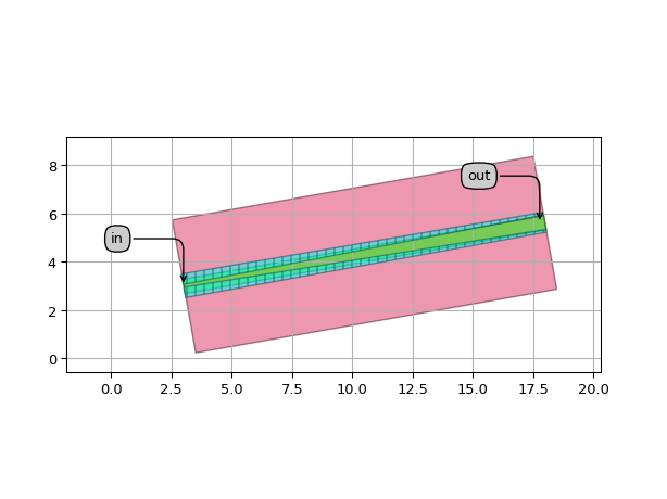
Wire Transitions
WireWaveguideTransitionLinear
- class picazzo3.traces.wire_wg.WireWaveguideTransitionLinear
A transition between two WireWaveguideTemplates.
- Parameters:
- end_trace_template: PCell and _TraceTemplate and WireWaveguideTemplate
- start_trace_template: PCell and _TraceTemplate and WireWaveguideTemplate
- name: String that contains only ISO/IEC 8859-1 (extended ASCII py3) or pure ASCII (py2) characters
The unique name of the pcell
- Other Parameters:
- reverse_templates: ( bool, bool_ or int ), locked
When True, treat start_trace_template as end_trace_template and vice versa. To use the correct templates, use the _{start/stop}_trace_template properties. This should not be set manually, but calculated by the transition itself.
Views
- class Layout
- Parameters:
- straight_extension: Coord2 and number >= 0
tuple: straight extension at start and end of transition
- end_position: Coord2
end position of the transition
- start_position: Coord2
start position of the transition
- view_name: String that contains only alphanumeric characters from the ASCII set or contains _$. ASCII set is extended on PY3.
The name of the view
- Other Parameters:
- length: float and Real, number and number >= 0, locked
length of the transition
Examples
"""This example shows how you use the template as a parameter for a rounded
Waveguide PCell."""
from picazzo3.traces.wire_wg import WireWaveguideTemplate
from picazzo3.traces.wire_wg import WireWaveguideTransitionLinear

wt1 = WireWaveguideTemplate()
wt1.Layout(core_width=0.45, cladding_width=1.6)
wt2 = WireWaveguideTemplate()
wt2.Layout(core_width=0.85, cladding_width=2.0)

t = WireWaveguideTransitionLinear(start_trace_template=wt1, end_trace_template=wt2)

t_lay = t.Layout(start_position=(0.0, 0.0), end_position=(5.0, 0.0))
t_lay.visualize(annotate=True)
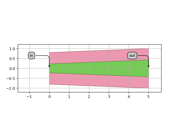
WireWaveguideTransitionFromPortLinear
- class picazzo3.traces.wire_wg.WireWaveguideTransitionFromPortLinear
A linear transition between two WireWaveguideTemplates.
- Parameters:
- start_port: _PortInterface
the port on which to extract trace template, position and angle
- end_trace_template: PCell and _TraceTemplate and WireWaveguideTemplate
- start_trace_template: PCell and _TraceTemplate and WireWaveguideTemplate
- name: String that contains only ISO/IEC 8859-1 (extended ASCII py3) or pure ASCII (py2) characters
The unique name of the pcell
- Other Parameters:
- reverse_templates: ( bool, bool_ or int ), locked
When True, treat start_trace_template as end_trace_template and vice versa. To use the correct templates, use the _{start/stop}_trace_template properties. This should not be set manually, but calculated by the transition itself.
Views
- class Layout
- Parameters:
- straight_extension: Coord2 and number >= 0
tuple: straight extension at start and end of transition
- length: float and Real, number and number >= 0
length of the transition
- end_position: Coord2
end position of the transition
- start_position: Coord2
start position of the transition
- view_name: String that contains only alphanumeric characters from the ASCII set or contains _$. ASCII set is extended on PY3.
The name of the view
Examples
"""This example shows how to append a transition onto a component.

We define a PCell with a port on the Layout level (position + angle). Then we use
WireWaveguideTransitionFromPortLinear to connect this port to a transition that creates
a transition to a wire waveguide.
"""
import si_fab.all as pdk  # noqa: F401
from ipkiss3 import all as i3
from picazzo3.traces.wire_wg import WireWaveguideTemplate, WireWaveguideTransitionFromPortLinear

wg_start = WireWaveguideTemplate()
wg_start.Layout(core_width=0.45, cladding_width=0.45 + 2 * i3.TECH.WG.TRENCH_WIDTH)

wg_end = WireWaveguideTemplate()
wg_end.Layout(core_width=2.0, cladding_width=2.0 + 2 * i3.TECH.WG.TRENCH_WIDTH)

p = i3.OpticalPort(name="out", position=(5.0, 0.0), angle=20.0, trace_template=wg_start)

t = WireWaveguideTransitionFromPortLinear(start_port=p, end_trace_template=wg_end)

t_lay = t.Layout(length=15.0, straight_extension=(0.5, 1.0))

t_lay.visualize(annotate=True)
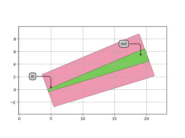
Waveguides
Bends
WgBend
- class picazzo3.wg.bend.cell.WgBend
Fixed Waveguide bend of an arbitrary angle. This is a rounded waveguide, so it takes a rounding algorithm and a bend radius as a parameter, as well as a trace_template.
- Parameters:
- trace_template: PCell and _WaveguideTemplate
- external_port_names: str
Dictionary for remapping of the port names of the contents to the external ports
- name: String that contains only ISO/IEC 8859-1 (extended ASCII py3) or pure ASCII (py2) characters
The unique name of the pcell
- Other Parameters:
- contents: PCell and _Trace, locked
Views
- class Layout
- Parameters:
- angle: float
angular coverage of the bend
- start_angle: float
start_angle of the bend. Negative is clockwise, positive is counterclockwise
- output_port: TracePort
- trace_template_for_ports: _TraceTemplate.Layout
Trace template to be used for the ports.
- shape: Shape
Shape from which the Trace is calculated
- cover_layers: List with type restriction, allowed types: <class ‘ipkiss.primitives.layer.Layer’>
layers that can be used to generate additional coverage of the trace (e.g. manhattan corners)
- reverse_individual_bends: list<( bool, bool_ or int )>
When set to True, it will generate the individual bends backwards. This has only effect when the bend algorithm is not symmetric. Should have length equal to the shape for closed shapes, but equal to shape-2 for open shapes.
- rounding_algorithms:
Rounding algorithm for every individual bend. Can be circular, spline, … Should have length equal to the shape for closed shapes, but equal to shape-2 for open shapes.
- bend_radii: list<number > 0>
Bend radius for every individual bend.
- reverse_bends: ( bool, bool_ or int )
When set to True, it will generate the bends backwards. This has only effect when the bend algorithm is not symmetric.
- remove_straight_angles: ( bool, bool_ or int )
Removes the waypoints with straight angles. Set to False if the algorithm uses waypoint-specific information.
- core_layer: __Layer__
layer used to define the core of the waveguide
- input_port: TracePort
- control_shape_layer: __Layer__
layer on which the control shape is drawn
- draw_control_shape: ( bool, bool_ or int )
draws the control shape on top of the waveguide
- contents_transformation: GenericNoDistortTransform
transformation to apply to the contents
- flatten_contents: ( bool, bool_ or int )
if True, it will insert the contents as elements in the layout, rather than as an Instance
- view_name: String that contains only alphanumeric characters from the ASCII set or contains _$. ASCII set is extended on PY3.
The name of the view
- manhattan: ( bool, bool_ or int )
Adds rectangular blocks in the bends to avoid as much as possible non-manhattan angles.
- angle_step: float and number > 0
Angle step for rounding.
- rounding_algorithm:
Rounding algorithm used to generate the bends. Can be circular, spline, ….
- bend_radius: float and number > 0
Bend radius for the auto-generated bends.
- Other Parameters:
- center_line_shape: locked
Automatically calculated shape of the center line of the trace
Examples
import si_fab.all as pdk  # noqa: F401
from picazzo3.wg.bend import WgBend
from picazzo3.traces.wire_wg.trace import WireWaveguideTemplate
import ipkiss3.all as i3

wg_t = WireWaveguideTemplate()
wg_t.Layout(core_width=0.550, cladding_width=i3.TECH.WG.CLADDING_WIDTH, core_process=i3.TECH.PROCESS.WG)
C = WgBend(trace_template=wg_t)
layout = C.Layout(bend_radius=20.0, start_angle=45.0, angle=-120)
layout.visualize(annotate=True)
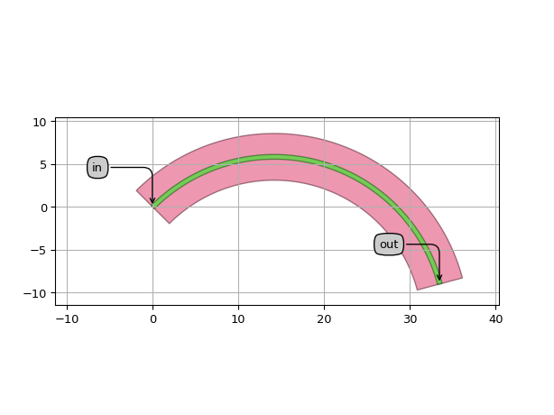
WgBend90
- class picazzo3.wg.bend.cell.WgBend90
Fixed Waveguide bend of 90 degrees. This is a rounded waveguide, so it takes a rounding algorithm and a bend radius as a parameter, as well as a trace_template.
- Parameters:
- trace_template: PCell and _WaveguideTemplate
- external_port_names: str
Dictionary for remapping of the port names of the contents to the external ports
- name: String that contains only ISO/IEC 8859-1 (extended ASCII py3) or pure ASCII (py2) characters
The unique name of the pcell
- Other Parameters:
- contents: PCell and _Trace, locked
Views
- class Layout
- Parameters:
- clockwise: ( bool, bool_ or int )
clockwise or counterclockwise propagation. By default it is calculated from ‘quadrant’
- quadrant: int and List with value restriction, allowed values: (-4, -3, -2, -1, 1, 2, 3, 4)
quadrant on the circle. (-4=>4)positive numbers is counterclockwise, negative numbers is clockwise
- start_angle: float
start_angle of the bend. By default it is calculated from ‘quadrant’
- output_port: TracePort
- trace_template_for_ports: _TraceTemplate.Layout
Trace template to be used for the ports.
- shape: Shape
Shape from which the Trace is calculated
- cover_layers: List with type restriction, allowed types: <class ‘ipkiss.primitives.layer.Layer’>
layers that can be used to generate additional coverage of the trace (e.g. manhattan corners)
- reverse_individual_bends: list<( bool, bool_ or int )>
When set to True, it will generate the individual bends backwards. This has only effect when the bend algorithm is not symmetric. Should have length equal to the shape for closed shapes, but equal to shape-2 for open shapes.
- rounding_algorithms:
Rounding algorithm for every individual bend. Can be circular, spline, … Should have length equal to the shape for closed shapes, but equal to shape-2 for open shapes.
- bend_radii: list<number > 0>
Bend radius for every individual bend.
- reverse_bends: ( bool, bool_ or int )
When set to True, it will generate the bends backwards. This has only effect when the bend algorithm is not symmetric.
- remove_straight_angles: ( bool, bool_ or int )
Removes the waypoints with straight angles. Set to False if the algorithm uses waypoint-specific information.
- core_layer: __Layer__
layer used to define the core of the waveguide
- input_port: TracePort
- control_shape_layer: __Layer__
layer on which the control shape is drawn
- draw_control_shape: ( bool, bool_ or int )
draws the control shape on top of the waveguide
- contents_transformation: GenericNoDistortTransform
transformation to apply to the contents
- flatten_contents: ( bool, bool_ or int )
if True, it will insert the contents as elements in the layout, rather than as an Instance
- view_name: String that contains only alphanumeric characters from the ASCII set or contains _$. ASCII set is extended on PY3.
The name of the view
- manhattan: ( bool, bool_ or int )
Adds rectangular blocks in the bends to avoid as much as possible non-manhattan angles.
- angle_step: float and number > 0
Angle step for rounding.
- rounding_algorithm:
Rounding algorithm used to generate the bends. Can be circular, spline, ….
- bend_radius: float and number > 0
Bend radius for the auto-generated bends.
- Other Parameters:
- angle: locked
angle of the bend (locked at 90 degrees)
- center_line_shape: locked
Automatically calculated shape of the center line of the trace
Examples
import si_fab.all as pdk  # noqa: F401
from picazzo3.wg.bend import WgBend90
from picazzo3.traces.wire_wg.trace import WireWaveguideTemplate
import ipkiss3.all as i3

wg_t = WireWaveguideTemplate()
wg_t.Layout(core_width=0.550, cladding_width=i3.TECH.WG.CLADDING_WIDTH, core_process=i3.TECH.PROCESS.WG)
C = WgBend90(trace_template=wg_t)
layout = C.Layout(quadrant=-3, bend_radius=20.0)
layout.visualize(annotate=True)
Crossings
WgDirectCrossing
- class picazzo3.wg.crossing.cell.WgDirectCrossing
A Direct waveguide crossing, consisting of two identical waveguides at right angles. This design is not particularly efficient for high-contrast waveguides, but is OK for low-contrast waveguides (e.g. silica.)
- Parameters:
- waveguides: List with type restriction, allowed types: <class ‘ipkiss3.pcell.cell.pcell.PCell’>
the waveguides through the crossing
- trace_template: PCell and _WaveguideTemplate
Trace template used to define the crossing
- name: String that contains only ISO/IEC 8859-1 (extended ASCII py3) or pure ASCII (py2) characters
The unique name of the pcell
Views
- class Layout
- Parameters:
- straight_stub: float and number > 0
length of the straight sections of the crossing
- length: float and number > 0
- view_name: String that contains only alphanumeric characters from the ASCII set or contains _$. ASCII set is extended on PY3.
The name of the view
Examples
import si_fab.all as pdk  # noqa: F401
from ipkiss3 import all as i3
from picazzo3.wg.crossing import WgDirectCrossing
from picazzo3.traces.wire_wg.trace import WireWaveguideTemplate

wg_t = WireWaveguideTemplate(name="my_crossing_wg_template1")
wg_t.Layout(core_width=0.550, cladding_width=2 * 2.0 + 0.550, core_process=i3.TECH.PROCESS.WG)
C = WgDirectCrossing(name="my_direct_crossing", trace_template=wg_t)
layout = C.Layout()

layout.visualize(annotate=True)
WgParabolicCrossing
- class picazzo3.wg.crossing.cell.WgParabolicCrossing
Highly efficient crossing for high-contrast silicon photonics. The crossing consists of double-etched parabolic transitions at right angles, collimating the optical field over a short distance to a parallel beam at the center of the crossing. This allows for a minimum of crosstalk. The details of this crossing are described in detail in [W. Bogaerts et al., Optics Letters, 32(19), p.2801-2803 (2007)]
- Parameters:
- waveguides: List with type restriction, allowed types: <class ‘ipkiss3.pcell.cell.pcell.PCell’>
the waveguides through the crossing
- trace_template: PCell and _WaveguideTemplate
Trace template used to define the crossing
- name: String that contains only ISO/IEC 8859-1 (extended ASCII py3) or pure ASCII (py2) characters
The unique name of the pcell
Views
- class Layout
- Parameters:
- core_width: float and number > 0
width of the shallow waveguide etch at the ports. defaults to same value as deep waveguide
- width_step: float and number > 0
discretisation in width for the parabolic shapes
- core_cladding_purpose: PatternPurpose
pattern purpose for the shallow etched core cladding
- cladding_purpose: PatternPurpose
pattern purpose for the full etched strip cladding
- core_purpose: PatternPurpose
pattern purpose for the shallow etched core
- strip_purpose: PatternPurpose
pattern purpose for the full etched strip
- core_cladding_process: ProcessLayer
process for the shallow etched core cladding
- cladding_process: ProcessLayer
process for the full etched strip cladding
- core_process: ProcessLayer
process for the shallow etched core
- strip_process: ProcessLayer
process for the full etched strip
- core_cladding_width: float and number > 0
width of the cladding of the shallow etched core
- core_width_center: float and number > 0
shallowetched core width at the center
- strip_width_center: float and number > 0
full etched strip width at the center
- straight_stub: float and number > 0
length of the straight sections of the crossing
- length: float and number > 0
length of the parabolic section (from start to crossing center to the end)
- view_name: String that contains only alphanumeric characters from the ASCII set or contains _$. ASCII set is extended on PY3.
The name of the view
Examples
import si_fab.all as pdk  # noqa: F401
from picazzo3.wg.crossing import WgParabolicCrossing

C = WgParabolicCrossing(name="my_parabolic_crossing")
layout = C.Layout(
    length=5.7, strip_width_center=2.6, core_width_center=0.8, core_cladding_width=2 * 0.5 + 0.8
)

layout.visualize(annotate=True)
Gratings
WaveguideUniformGrating
- class picazzo3.wg.grating.cell.WaveguideUniformGrating
Waveguide with inline, uniform grating. The grating consists of a Child cell with the period, which is repeated to create the grating.
- Parameters:
- n_o_periods: int and number > 0
The number of periods
- period_cell: PCell and _WaveguideGratingPeriod
The unit cell of the grating
- name: String that contains only ISO/IEC 8859-1 (extended ASCII py3) or pure ASCII (py2) characters
The unique name of the pcell
Views
- class Layout
- Parameters:
- view_name: String that contains only alphanumeric characters from the ASCII set or contains _$. ASCII set is extended on PY3.
The name of the view
Examples
"""How to create a uniform grating with a custom unit cell."""
import si_fab.all as pdk  # noqa: F401
from picazzo3.wg.grating import WaveguideUniformGrating, WaveguideSectionsGratingPeriod
from picazzo3.traces.wire_wg import WireWaveguideTemplate
from picazzo3.traces.slot_wg import SlotWaveguideTemplate

# 2 templates to make a single period
t1 = WireWaveguideTemplate(name="wire_t")
t1.Layout(core_width=0.6, cladding_width=3.0)

t2 = SlotWaveguideTemplate(name="slot_t")
t2.Layout(core_width=0.6, slot_width=0.15, cladding_width=3.0)

period = WaveguideSectionsGratingPeriod(name="period", wg_templates=[t1, t2, t1])
period.Layout(section_lengths=[0.11, 0.5, 0.11])

grating = WaveguideUniformGrating(name="my_uniform_grating", period_cell=period, n_o_periods=12)
layout = grating.Layout()

layout.visualize(annotate=True)

WaveguideNonUniformGrating
- class picazzo3.wg.grating.cell.WaveguideNonUniformGrating
Waveguide with inline, non-uniform grating. The grating periods are described as individual cells, and they are concatenated into a grating.
- Parameters:
- period_cells: List with type restriction, allowed types: <class ‘ipkiss3.pcell.cell.pcell.PCell’> and List with type restriction, allowed types: <class ‘picazzo3.wg.grating.cell._WaveguideGratingPeriod’>
- name: String that contains only ISO/IEC 8859-1 (extended ASCII py3) or pure ASCII (py2) characters
The unique name of the pcell
Views
- class Layout
- Parameters:
- view_name: String that contains only alphanumeric characters from the ASCII set or contains _$. ASCII set is extended on PY3.
The name of the view
Examples
"""How to create a fully customized non-uniform grating using
3 different unit cells constructed from two waveguide templates.
"""

import si_fab.all as pdk  # noqa: F401
from picazzo3.wg.grating import WaveguideNonUniformGrating, WaveguideSectionsGratingPeriod
from picazzo3.traces.wire_wg import WireWaveguideTemplate
from picazzo3.traces.slot_wg import SlotWaveguideTemplate

# 2 templates to make a single period unit cell
t1 = WireWaveguideTemplate(name="wire_t")
t1.Layout(core_width=0.6, cladding_width=3.0)

t2 = SlotWaveguideTemplate(name="slot_t")
t2.Layout(core_width=0.6, slot_width=0.15, cladding_width=3.0)

# 3 different grating period unit cells
period1 = WaveguideSectionsGratingPeriod(name="period1", wg_templates=[t1, t2, t1])
period1.Layout(section_lengths=[0.2, 0.3, 0.2])

period2 = WaveguideSectionsGratingPeriod(name="period2", wg_templates=[t1, t2, t1])
period2.Layout(section_lengths=[0.13, 0.4, 0.13])

period3 = WaveguideSectionsGratingPeriod(name="period3", wg_templates=[t1, t2, t1])
period3.Layout(section_lengths=[0.11, 0.5, 0.11])

# a nonuniform grating with different starting and ending cells (apodized)
grating = WaveguideNonUniformGrating(
    name="my_nonuniform_grating",
    period_cells=[
        period1,
        period2,
        period3,
        period3,
        period3,
        period3,
        period3,
        period3,
        period3,
        period3,
        period3,
        period3,
        period3,
        period3,
        period2,
        period1,
    ],
)
layout = grating.Layout()

layout.visualize(annotate=True)
ModifiedWaveguideGratingPeriod
- class picazzo3.wg.grating.cell.ModifiedWaveguideGratingPeriod
Period for a waveguide with modified parameters. The base definition is taken from the wg_template which is used for the ports. The modify_waveguide_parameters property then creates the blocks with modified widths, by adapting the properties of the individual waveguide template.
- Parameters:
- modified_waveguide_parameters: list
Dict of the parameters of the waveguide template that should be modified for the different sections of the Grating Period.
- n_o_sections: int and number > 0
Number of sections in the grating period
- wg_template: PCell and _WaveguideTemplate
Waveguide template of start and end of the period (and ports)
- name: String that contains only ISO/IEC 8859-1 (extended ASCII py3) or pure ASCII (py2) characters
The unique name of the pcell
- Other Parameters:
- wg_templates: List with type restriction, allowed types: <class ‘ipkiss3.pcell.cell.pcell.PCell’>, locked
Views
- class Layout
- Parameters:
- section_lengths: list<number >= 0>
List of lengths for the waveguide templates
- length: float and Real, number and number >= 0
Length of the grating period.
- view_name: String that contains only alphanumeric characters from the ASCII set or contains _$. ASCII set is extended on PY3.
The name of the view
Examples
"""In this example we build a grating from a modified slot waveguide.
Starting from the basic slot waveguide template, we define grating period sections
with different slot width and core width.
"""
import si_fab.all as pdk  # noqa: F401
from picazzo3.wg.grating import WaveguideUniformGrating, ModifiedWaveguideGratingPeriod
from picazzo3.traces.slot_wg import SlotWaveguideTemplate

t = SlotWaveguideTemplate(name="slot_t")
t.Layout(core_width=0.6, slot_width=0.15, cladding_width=3.0)

period = ModifiedWaveguideGratingPeriod(name="period", wg_template=t, n_o_sections=5)

# we modify the core width and the slot width
period.Layout(
    section_lengths=[0.1, 0.1, 0.3, 0.1, 0.1],
    modified_waveguide_parameters={
        "slot_width": [0.15, 0.18, 0.20, 0.18, 0.15],
        "core_width": [0.6, 0.59, 0.58, 0.59, 0.6],
    },
)

grating = WaveguideUniformGrating(name="my_grating_modifiedwg", period_cell=period, n_o_periods=12)
layout = grating.Layout()

layout.visualize(annotate=True)
WaveguideSideGratingPeriod
- class picazzo3.wg.grating.cell.WaveguideSideGratingPeriod
Period for a waveguide with side gratings. The base definition is taken from the wg_template which is used for the ports. The widths property then creates the blocks with modified widths, based on the original. (another parameter can be adapted by changing the property width_parameter_name)
- Parameters:
- n_o_sections: int and number > 0
Number of sections in the grating period
- wg_template: PCell and _WaveguideTemplate
Waveguide template of start and end of the period (and ports)
- name: String that contains only ISO/IEC 8859-1 (extended ASCII py3) or pure ASCII (py2) characters
The unique name of the pcell
- Other Parameters:
- modified_waveguide_parameters: locked
- wg_templates: List with type restriction, allowed types: <class ‘ipkiss3.pcell.cell.pcell.PCell’>, locked
Views
- class Layout
- Parameters:
- relative_widths: ( bool, bool_ or int )
If True, the values of the width are relative to the original value.
- width_parameter_name: String that contains only alphanumeric characters from the ASCII set or contains _$. ASCII set is extended on PY3.
Name of the property of the waveguide template that is to be adjusted by the values in ‘widths’.
- widths: list<Real, number>
The modified widths of the waveguide core. If ‘relative_widths’ is True, the values are relative to the original core width. It is also possible to adjust another parameter than ‘core_width’ by overriding the ‘width_parameter_name’.
- section_lengths: list<number >= 0>
List of lengths for the waveguide templates
- length: float and Real, number and number >= 0
Length of the grating period.
- view_name: String that contains only alphanumeric characters from the ASCII set or contains _$. ASCII set is extended on PY3.
The name of the view
Examples
"""We make a grating based on a wire waveguide and modify the width of the core
to create side gratings:
"""
import si_fab.all as pdk  # noqa: F401
from picazzo3.wg.grating import WaveguideUniformGrating, WaveguideSideGratingPeriod

period = WaveguideSideGratingPeriod(n_o_sections=3)

# we modify the width with +/- 50nm
# relative to the original core width
period.Layout(section_lengths=[0.1, 0.13, 0.1], widths=[-0.05, +0.05, -0.05], relative_widths=True)

grating = WaveguideUniformGrating(name="my_side_grating", period_cell=period, n_o_periods=12)
layout = grating.Layout()

layout.visualize(annotate=True)
Directional Couplers
StraightDirectionalCoupler
- class picazzo3.wg.dircoup.cell.StraightDirectionalCoupler
A directional coupler consisting of 2 parallel (horizontal) straight waveguides.
- Parameters:
- wg2b: PCell
North-east waveguide
- wg2a: PCell
North-west waveguide
- wg1b: PCell
South-east waveguide
- wg1a: PCell
South-west waveguide
- trace_template2: PCell and _WaveguideTemplate
waveguide template used by the north arm of the directional coupler. If not set, it defaults to the template of the south arm
- trace_template1: PCell and _WaveguideTemplate
waveguide template used by the south arm of the directional coupler
- coupler_length: float and Real, number and number >= 0
length of the directional coupler
- name: String that contains only ISO/IEC 8859-1 (extended ASCII py3) or pure ASCII (py2) characters
The unique name of the pcell
- Other Parameters:
- n_inputs: int and number > 0, locked
Number of input channels.
- n_outputs: int and number > 0, locked
Number of output channels.
Views
- class Layout
- Parameters:
- straight_extensions: Coord2 and number >= 0
additional lengths of the couplers at start and end
- wg2b_shape: Shape
Shape for the north-east part of the waveguide
- wg2a_shape: Shape
Shape for the north-west part of the waveguide
- wg1b_shape: Shape
Shape for the south-east part of the waveguide
- wg1a_shape: Shape
Shape for the south-west part of the waveguide
- coupler_spacing: float
Spacing between the two waveguide centerlines.
- view_name: String that contains only alphanumeric characters from the ASCII set or contains _$. ASCII set is extended on PY3.
The name of the view
Examples
import si_fab.all as pdk  # noqa: F401
from ipkiss3 import all as i3
from picazzo3.wg.dircoup import StraightDirectionalCoupler
from picazzo3.traces.wire_wg.trace import WireWaveguideTemplate

wg_t = WireWaveguideTemplate(name="my_wg_template1")
wg_t.Layout(core_width=0.550, cladding_width=i3.TECH.WG.CLADDING_WIDTH, core_process=i3.TECH.PROCESS.WG)

C = StraightDirectionalCoupler(name="my_dircoup1", trace_template1=wg_t, coupler_length=6.0)
layout = C.Layout(coupler_spacing=0.7)

layout.visualize(annotate=True)
BendDirectionalCoupler
- class picazzo3.wg.dircoup.cell.BendDirectionalCoupler
A directional coupler consisting of 2 parallel (horizontal) waveguides with bends at the start and end.
- Parameters:
- wg2b: PCell
North-east waveguide
- wg2a: PCell
North-west waveguide
- wg1b: PCell
South-east waveguide
- wg1a: PCell
South-west waveguide
- trace_template2: PCell and _WaveguideTemplate
waveguide template used by the north arm of the directional coupler. If not set, it defaults to the template of the south arm
- trace_template1: PCell and _WaveguideTemplate
waveguide template used by the south arm of the directional coupler
- coupler_length: float and Real, number and number >= 0
length of the directional coupler
- name: String that contains only ISO/IEC 8859-1 (extended ASCII py3) or pure ASCII (py2) characters
The unique name of the pcell
- Other Parameters:
- n_inputs: int and number > 0, locked
Number of input channels.
- n_outputs: int and number > 0, locked
Number of output channels.
Views
- class Layout
- Parameters:
- bend_angles2: tuple2
Input and output angle of the bends of arm 2. Defaults to bend_angle. If set, bend_angle will be ignored.
- bend_angles1: tuple2
Input and output angle of the bends of arm 1. Defaults to bend_angle. If set, bend_angle will be ignored.
- straight_after_bend: float and Real, number and number >= 0
length of the straight waveguide after the bend
- bend_angle: float
angle at which the directional coupler is bent
- reverse_individual_bends2b: List with type restriction, allowed types: <class ‘bool’>
List of booleans to indicate whether the individual bends in arm2 should be reversed
- reverse_individual_bends1b: List with type restriction, allowed types: <class ‘bool’>
List of booleans to indicate whether the individual bends in arm1 should be reversed
- reverse_individual_bends2a: List with type restriction, allowed types: <class ‘bool’>
List of booleans to indicate whether the individual bends in arm2 should be reversed
- reverse_individual_bends1a: List with type restriction, allowed types: <class ‘bool’>
List of booleans to indicate whether the individual bends in arm1 should be reversed
- reverse_bends: ( bool, bool_ or int )
If True, all bends will be reversed. This has only an effect on asymmetric bends, such as splines
- wg2b_shape: Shape
Shape for the north-east part of the waveguide
- wg2a_shape: Shape
Shape for the north-west part of the waveguide
- wg1b_shape: Shape
Shape for the south-east part of the waveguide
- wg1a_shape: Shape
Shape for the south-west part of the waveguide
- coupler_spacing: float
Spacing between the two waveguide centerlines.
- view_name: String that contains only alphanumeric characters from the ASCII set or contains _$. ASCII set is extended on PY3.
The name of the view
- manhattan: ( bool, bool_ or int )
Adds rectangular blocks in the bends to avoid as much as possible non-manhattan angles.
- angle_step: float and number > 0
Angle step for rounding.
- rounding_algorithm:
Rounding algorithm used to generate the bends. Can be circular, spline, ….
- bend_radius: float and number > 0
Bend radius for the auto-generated bends.
Examples
import si_fab.all as pdk  # noqa: F401
from picazzo3.wg.dircoup import BendDirectionalCoupler
from picazzo3.traces.wire_wg.trace import WireWaveguideTemplate
import ipkiss3.all as i3

wg_t = WireWaveguideTemplate(name="my_wg_template2")
wg_t.Layout(core_width=0.500, cladding_width=i3.TECH.WG.CLADDING_WIDTH, core_process=i3.TECH.PROCESS.WG)
C = BendDirectionalCoupler(name="my_dircoup_2", trace_template1=wg_t, coupler_length=6.0)
layout = C.Layout(
    coupler_spacing=0.7, bend_radius=10.0, manhattan=True, straight_after_bend=6.0, bend_angle=60.0
)
layout.visualize(annotate=True)
SBendDirectionalCoupler
- class picazzo3.wg.dircoup.cell.SBendDirectionalCoupler
A directional coupler consisting of 2 parallel (horizontal) waveguides with S-shaped bends at the start and end.
- Parameters:
- wg2b: PCell
North-east waveguide
- wg2a: PCell
North-west waveguide
- wg1b: PCell
South-east waveguide
- wg1a: PCell
South-west waveguide
- trace_template2: PCell and _WaveguideTemplate
waveguide template used by the north arm of the directional coupler. If not set, it defaults to the template of the south arm
- trace_template1: PCell and _WaveguideTemplate
waveguide template used by the south arm of the directional coupler
- coupler_length: float and Real, number and number >= 0
length of the directional coupler
- name: String that contains only ISO/IEC 8859-1 (extended ASCII py3) or pure ASCII (py2) characters
The unique name of the pcell
- Other Parameters:
- n_inputs: int and number > 0, locked
Number of input channels.
- n_outputs: int and number > 0, locked
Number of output channels.
Views
- class Layout
- Parameters:
- sbend_straight: float and Real, number and number >= 0
length of the straight section in the S-bend
- bend_angles2: tuple2
Input and output angle of the bends of arm 2. Defaults to bend_angle. If set, bend_angle will be ignored.
- bend_angles1: tuple2
Input and output angle of the bends of arm 1. Defaults to bend_angle. If set, bend_angle will be ignored.
- straight_after_bend: float and Real, number and number >= 0
length of the straight waveguide after the bend
- bend_angle: float
angle at which the directional coupler is bent
- reverse_individual_bends2b: List with type restriction, allowed types: <class ‘bool’>
List of booleans to indicate whether the individual bends in arm2 should be reversed
- reverse_individual_bends1b: List with type restriction, allowed types: <class ‘bool’>
List of booleans to indicate whether the individual bends in arm1 should be reversed
- reverse_individual_bends2a: List with type restriction, allowed types: <class ‘bool’>
List of booleans to indicate whether the individual bends in arm2 should be reversed
- reverse_individual_bends1a: List with type restriction, allowed types: <class ‘bool’>
List of booleans to indicate whether the individual bends in arm1 should be reversed
- reverse_bends: ( bool, bool_ or int )
If True, all bends will be reversed. This has only an effect on asymmetric bends, such as splines
- wg2b_shape: Shape
Shape for the north-east part of the waveguide
- wg2a_shape: Shape
Shape for the north-west part of the waveguide
- wg1b_shape: Shape
Shape for the south-east part of the waveguide
- wg1a_shape: Shape
Shape for the south-west part of the waveguide
- coupler_spacing: float
Spacing between the two waveguide centerlines.
- view_name: String that contains only alphanumeric characters from the ASCII set or contains _$. ASCII set is extended on PY3.
The name of the view
- manhattan: ( bool, bool_ or int )
Adds rectangular blocks in the bends to avoid as much as possible non-manhattan angles.
- angle_step: float and number > 0
Angle step for rounding.
- rounding_algorithm:
Rounding algorithm used to generate the bends. Can be circular, spline, ….
- bend_radius: float and number > 0
Bend radius for the auto-generated bends.
Examples
import si_fab.all as pdk  # noqa: F401
from picazzo3.wg.dircoup import SBendDirectionalCoupler
from picazzo3.traces.wire_wg.trace import WireWaveguideTemplate
import ipkiss3.all as i3

wg_t = WireWaveguideTemplate()
wg_t.Layout(core_width=0.500, cladding_width=i3.TECH.WG.CLADDING_WIDTH, core_process=i3.TECH.PROCESS.WG)

C = SBendDirectionalCoupler(name="my_sbenddircoup3", trace_template1=wg_t, coupler_length=6.0)
layout = C.Layout(coupler_spacing=0.7, straight_after_bend=6.0, bend_angle=30.0)
layout.visualize(annotate=True)
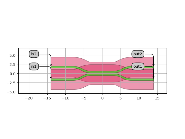
"""A more complicated example using asymmetric spline bends and different
waveguide definition in the two arms.
"""
import si_fab.all as pdk  # noqa: F401
from picazzo3.wg.dircoup import SBendDirectionalCoupler
from picazzo3.traces.wire_wg.trace import WireWaveguideTemplate
from ipkiss3.all import SplineRoundingAlgorithm
import ipkiss3.all as i3

wg_t = WireWaveguideTemplate(name="my_wg_template4")
wg_t.Layout(core_width=0.500, cladding_width=i3.TECH.WG.CLADDING_WIDTH, core_process=i3.TECH.PROCESS.WG)

wg_t2 = WireWaveguideTemplate(name="my_wg_template5")
wg_t2.Layout(
    core_width=0.600, cladding_width=i3.TECH.WG.CLADDING_WIDTH, core_process=i3.TECH.PROCESS.WG
)

ra = SplineRoundingAlgorithm(adiabatic_angles=(30.0, 0))  # asymmetric

C = SBendDirectionalCoupler(
    name="my_sbenddircoup_4", trace_template1=wg_t, trace_template2=wg_t2, coupler_length=6.0
)

layout = C.Layout(
    coupler_spacing=0.7,
    bend_radius=5.0,
    manhattan=True,
    straight_after_bend=6.0,
    sbend_straight=1.0,
    bend_angle=30.0,
    rounding_algorithm=ra,
)
layout.visualize(annotate=True)
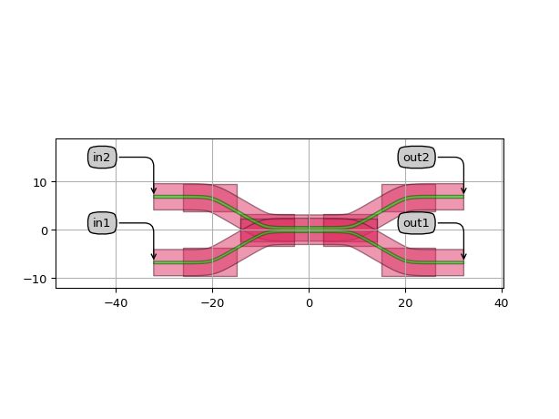
Splitters
WgYSplitter
- class picazzo3.wg.splitters.cell.WgYSplitter
Y-splitter PCell with branches that fan out specifiable angle.
- Parameters:
- trace_template: PCell and _WaveguideTemplate
Waveguide template of the Y splitter
- name: String that contains only ISO/IEC 8859-1 (extended ASCII py3) or pure ASCII (py2) characters
The unique name of the pcell
Views
- class Layout
- Parameters:
- split_stub_width: float and number > 0
Width of the stub where the waveguide split
- center_waveguide_length: float and Real, number and number >= 0
Length of the center waveguide
- taper_length: float and Real, number and number >= 0
Length of the tapered section
- angle_out: float
Angle at which the waveguide exit the splitter.
- cladding_width: float and number > 0
Width of the cladding. The default is taken from the trace template.
- core_width: float and number > 0
Width of the core. The default is taken from the trace template.
- bend_radius: float and number > 0
- view_name: String that contains only alphanumeric characters from the ASCII set or contains _$. ASCII set is extended on PY3.
The name of the view
Examples
import si_fab.all as pdk  # noqa: F401
from picazzo3.wg.splitters import WgYSplitter

C = WgYSplitter(name="my_splitter90")
layout = C.Layout(bend_radius=4.5, angle_out=60.0)

layout.visualize(annotate=True)
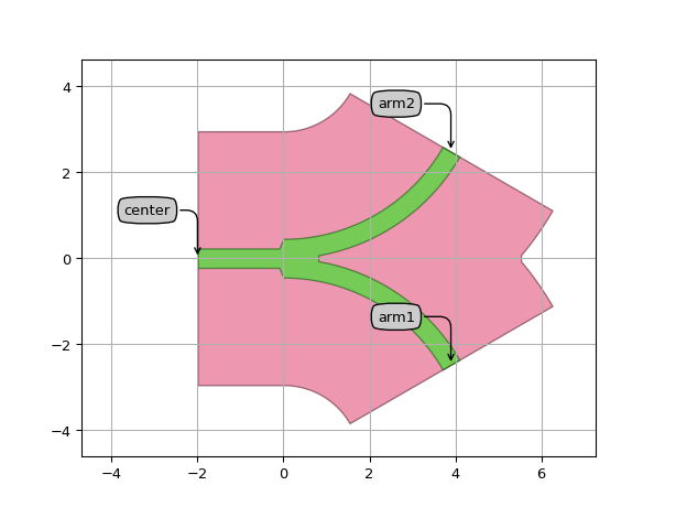
WgYCombiner
- class picazzo3.wg.splitters.cell.WgYCombiner
Y-Combiner PCell with branches that fan out specifiable angle.
- Parameters:
- trace_template: PCell and _WaveguideTemplate
Waveguide template of the Y splitter
- name: String that contains only ISO/IEC 8859-1 (extended ASCII py3) or pure ASCII (py2) characters
The unique name of the pcell
Views
- class Layout
- Parameters:
- split_stub_width: float and number > 0
Width of the stub where the waveguide split
- center_waveguide_length: float and Real, number and number >= 0
Length of the center waveguide
- taper_length: float and Real, number and number >= 0
Length of the tapered section
- angle_out: float
Angle at which the waveguide exit the splitter.
- cladding_width: float and number > 0
Width of the cladding. The default is taken from the trace template.
- core_width: float and number > 0
Width of the core. The default is taken from the trace template.
- bend_radius: float and number > 0
- view_name: String that contains only alphanumeric characters from the ASCII set or contains _$. ASCII set is extended on PY3.
The name of the view
Examples
import si_fab.all as pdk  # noqa: F401
from picazzo3.wg.splitters import WgYCombiner

C = WgYCombiner(name="my_combiner60")
layout = C.Layout(bend_radius=4.5, core_width=0.6, angle_out=60.0)
layout.visualize(annotate=True)
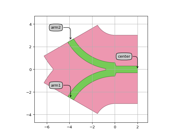
WgY90Splitter
- class picazzo3.wg.splitters.cell.WgY90Splitter
Y-splitter PCell with branches that fan out at right angles to the input waveguide.
- Parameters:
- trace_template: PCell and _WaveguideTemplate
Waveguide template of the Y splitter
- name: String that contains only ISO/IEC 8859-1 (extended ASCII py3) or pure ASCII (py2) characters
The unique name of the pcell
Views
- class Layout
- Parameters:
- split_stub_width: float and number > 0
Width of the stub where the waveguide split
- center_waveguide_length: float and Real, number and number >= 0
Length of the center waveguide
- taper_length: float and Real, number and number >= 0
Length of the tapered section
- cladding_width: float and number > 0
Width of the cladding. The default is taken from the trace template.
- core_width: float and number > 0
Width of the core. The default is taken from the trace template.
- bend_radius: float and number > 0
- view_name: String that contains only alphanumeric characters from the ASCII set or contains _$. ASCII set is extended on PY3.
The name of the view
- Other Parameters:
- angle_out: float, locked
Angle at which the waveguide exit the splitter.
Examples
import si_fab.all as pdk  # noqa: F401
from picazzo3.wg.splitters import WgY90Splitter

C = WgY90Splitter(name="my_splitter90")
layout = C.Layout(bend_radius=4.5)

layout.visualize(annotate=True)
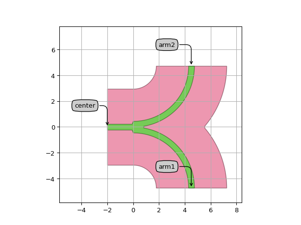
WgY90Combiner
- class picazzo3.wg.splitters.cell.WgY90Combiner
Y-shaped combiner with branches that come in at right angles to the output waveguide.
- Parameters:
- trace_template: PCell and _WaveguideTemplate
Waveguide template of the Y splitter
- name: String that contains only ISO/IEC 8859-1 (extended ASCII py3) or pure ASCII (py2) characters
The unique name of the pcell
Views
- class Layout
- Parameters:
- split_stub_width: float and number > 0
Width of the stub where the waveguide split
- center_waveguide_length: float and Real, number and number >= 0
Length of the center waveguide
- taper_length: float and Real, number and number >= 0
Length of the tapered section
- cladding_width: float and number > 0
Width of the cladding. The default is taken from the trace template.
- core_width: float and number > 0
Width of the core. The default is taken from the trace template.
- bend_radius: float and number > 0
- view_name: String that contains only alphanumeric characters from the ASCII set or contains _$. ASCII set is extended on PY3.
The name of the view
- Other Parameters:
- angle_out: float, locked
Angle at which the waveguide exit the splitter.
Examples
import si_fab.all as pdk  # noqa: F401
from picazzo3.wg.splitters import WgY90Combiner

C = WgY90Combiner(name="my_combiner90")
layout = C.Layout(bend_radius=4.5, core_width=0.6)

layout.visualize(annotate=True)
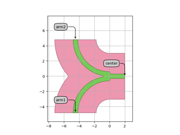
WgY180Splitter
- class picazzo3.wg.splitters.cell.WgY180Splitter
Y-splitter PCell with branches that fan out at right angles to the input waveguide and then come back to the horizontal direction.
- Parameters:
- trace_template: PCell and _WaveguideTemplate
Waveguide template of the Y splitter
- name: String that contains only ISO/IEC 8859-1 (extended ASCII py3) or pure ASCII (py2) characters
The unique name of the pcell
Views
- class Layout
- Parameters:
- bend_radius: float and number > 0
- view_name: String that contains only alphanumeric characters from the ASCII set or contains _$. ASCII set is extended on PY3.
The name of the view
Examples
import si_fab.all as pdk  # noqa: F401
from picazzo3.wg.splitters import WgY180Splitter

C = WgY180Splitter(name="my_splitter180")
layout = C.Layout(bend_radius=4.5)

layout.visualize(annotate=True)
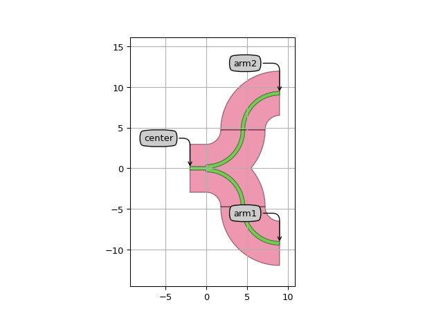
WgY180Combiner
- class picazzo3.wg.splitters.cell.WgY180Combiner
Y-shaped combiner with branches that come in horizontally and combine with the output waveguide at right angles.
- Parameters:
- trace_template: PCell and _WaveguideTemplate
Waveguide template of the Y splitter
- name: String that contains only ISO/IEC 8859-1 (extended ASCII py3) or pure ASCII (py2) characters
The unique name of the pcell
Views
- class Layout
- Parameters:
- bend_radius: float and number > 0
- view_name: String that contains only alphanumeric characters from the ASCII set or contains _$. ASCII set is extended on PY3.
The name of the view
Examples
import si_fab.all as pdk  # noqa: F401
from picazzo3.wg.splitters import WgY180Combiner

C = WgY180Combiner(name="my_combiner180")
layout = C.Layout(bend_radius=4.5)

layout.visualize(annotate=True)
Waveguide Bundles
WaveguideBundle
- class picazzo3.wg.bundle.cell.WaveguideBundle
Bundle of waveguides, routed together
- Parameters:
- traces: List with type restriction, allowed types: <class ‘ipkiss3.pcell.cell.pcell.PCell’>
the traces in this bundle
- name: String that contains only ISO/IEC 8859-1 (extended ASCII py3) or pure ASCII (py2) characters
The unique name of the pcell
Views
- class Layout
- Parameters:
- area_layer_on: ( bool, bool_ or int )
When True, the entire bundle area will be covered by all the cover layers.
- trace_transformations: list and List with type restriction, allowed types: <class ‘ipkiss.geometry.transform.Transform’>
transformations to be applied to each of the traces
- cover_layers: List with type restriction, allowed types: <class ‘ipkiss.primitives.layer.Layer’>
layers that can be used to generate additional coverage of the trace (e.g. manhattan corners)
- view_name: String that contains only alphanumeric characters from the ASCII set or contains _$. ASCII set is extended on PY3.
The name of the view
Examples
import si_fab.all as pdk  # noqa: F401
import ipkiss3.all as i3
from picazzo3.wg.bundle import WaveguideBundle
from picazzo3.traces.wire_wg.trace import WireWaveguideTemplate

wg_t = WireWaveguideTemplate()
wg_t.Layout(core_width=0.550, cladding_width=i3.TECH.WG.CLADDING_WIDTH, core_process=i3.TECH.PROCESS.WG)
trace = wg_t()
trace.Layout(shape=[(0.0, 0.0), (20.0, 5.0)])
trace_tfs = [i3.Translation(translation=(0.0, 10.0 * i)) for i in range(5)]
C = WaveguideBundle(traces=[trace] * 5)
lay = C.Layout(trace_transformations=trace_tfs)
lay.visualize(annotate=True)
#pcell: picazzo3.wg.bundle.cell.TemplatedWaveguideBundle#
Spirals
SingleSpiral
- class picazzo3.wg.spirals.cell.SingleSpiral
Single spiral class going from the inside to the outside. The trace template provided in the property
trace_templateis used to build a chain of waveguides.- Parameters:
- n_o_loops: int and number > 0
Number of loops in the spiral
- trace_template: PCell and _TraceTemplate
Trace template used in the chain.
- name: String that contains only ISO/IEC 8859-1 (extended ASCII py3) or pure ASCII (py2) characters
The unique name of the pcell
- Other Parameters:
- n_o_traces: int and number > 0, locked
Total number of traces used in the spiral.
- traces: List with type restriction, allowed types: <class ‘ipkiss3.pcell.cell.pcell.PCell’>, locked
Views
- class Layout
- Parameters:
- shapes: list
List of shapes used to build the traces
- flatten: ( bool, bool_ or int )
If true the instances are flattened
- inner_size: Coord2 and number >= 0
Inner size of the the spiral, defaults to 3 * spacing + 2 * bend_radius, in each direction
- view_name: String that contains only alphanumeric characters from the ASCII set or contains _$. ASCII set is extended on PY3.
The name of the view
- spacing: float and Real, number and number >= 0
spacing between the individual loops.
- spiral_center: Coord2
location of the center of the spiral.
- Other Parameters:
- auto_transform: locked
Examples
# Example of single spiral using a trace template.
import si_fab.all as pdk  # noqa: F401
from picazzo3.wg.spirals import SingleSpiral
from ipkiss3 import all as i3

cell = SingleSpiral(n_o_loops=5, trace_template=i3.TECH.PCELLS.WG.DEFAULT)
layout = cell.Layout(inner_size=(20, 15), spacing=5.0, spiral_center=(2, 1))

layout.visualize(annotate=True)
SingleSpiralRounded
- class picazzo3.wg.spirals.cell.SingleSpiralRounded
Rounded single spiral class going from the inside to the outside. The trace template provided in the property
trace_templateis used to build a chain of waveguides. All the rounding properties can be set at the layout level.- Parameters:
- n_o_loops: int and number > 0
Number of loops in the spiral
- trace_template: PCell and _TraceTemplate
Trace template used in the chain.
- name: String that contains only ISO/IEC 8859-1 (extended ASCII py3) or pure ASCII (py2) characters
The unique name of the pcell
- Other Parameters:
- n_o_traces: int and number > 0, locked
Total number of traces used in the spiral.
- traces: List with type restriction, allowed types: <class ‘ipkiss3.pcell.cell.pcell.PCell’>, locked
Views
- class Layout
- Parameters:
- shapes: list
List of shapes used to build the traces
- flatten: ( bool, bool_ or int )
If true the instances are flattened
- spacing: float and Real, number and number >= 0
spacing between the individual loops.
- spiral_center: Coord2
location of the center of the spiral.
- inner_size: Coord2 and number >= 0
Inner size of the the spiral, defaults to 3 * spacing + 2 * bend_radius, in each direction
- view_name: String that contains only alphanumeric characters from the ASCII set or contains _$. ASCII set is extended on PY3.
The name of the view
- manhattan: ( bool, bool_ or int )
Adds rectangular blocks in the bends to avoid as much as possible non-manhattan angles.
- angle_step: float and number > 0
Angle step for rounding.
- rounding_algorithm:
Rounding algorithm used to generate the bends. Can be circular, spline, ….
- bend_radius: float and number > 0
Bend radius for the auto-generated bends.
- Other Parameters:
- auto_transform: locked
Examples
import si_fab.all as pdk  # noqa: F401
from picazzo3.wg.spirals import SingleSpiralRounded
from ipkiss3 import all as i3

cell = SingleSpiralRounded(n_o_loops=5, trace_template=i3.TECH.PCELLS.WG.DEFAULT)
layout = cell.Layout(
    inner_size=(30.0, 30.0), bend_radius=3.0, manhattan=True, spacing=5.0, spiral_center=(2, 1)
)

layout.visualize(annotate=True)
DoubleSpiral
- class picazzo3.wg.spirals.cell.DoubleSpiral
Double spiral class with both access waveguides on the outside of the spiral. The trace template provided in the property
trace_templateis used to build a chain of waveguides.- Parameters:
- n_o_loops: int and number > 0
Number of loops in the spiral
- trace_template: PCell and _TraceTemplate
Trace template used in the chain.
- name: String that contains only ISO/IEC 8859-1 (extended ASCII py3) or pure ASCII (py2) characters
The unique name of the pcell
- Other Parameters:
- n_o_traces: int and number > 0, locked
Total number of traces used in the spiral.
- traces: List with type restriction, allowed types: <class ‘ipkiss3.pcell.cell.pcell.PCell’>, locked
Views
- class Layout
- Parameters:
- shapes: list
List of shapes used to build the traces
- flatten: ( bool, bool_ or int )
If true the instances are flattened
- inner_size: Coord2 and number >= 0
Inner size of the the spiral, defaults to 3 * spacing + 2 * bend_radius, in each direction
- view_name: String that contains only alphanumeric characters from the ASCII set or contains _$. ASCII set is extended on PY3.
The name of the view
- stub_direction: List with value restriction, allowed values: [‘H’, ‘V’]
- spacing: float and Real, number and number >= 0
spacing between the individual loops.
- spiral_center: Coord2
location of the center of the spiral.
- Other Parameters:
- auto_transform: locked
Examples
import si_fab.all as pdk  # noqa: F401
from picazzo3.wg.spirals import DoubleSpiral
from ipkiss3 import all as i3

cell = DoubleSpiral(n_o_loops=2, trace_template=i3.TECH.PCELLS.WG.DEFAULT)
layout = cell.Layout(
    inner_size=(15.0, 15.0), spacing=1.0, stub_direction="H", spiral_center=(0, 0)  # either H or V
)

layout.visualize(annotate=True)
DoubleSpiralRounded
- class picazzo3.wg.spirals.cell.DoubleSpiralRounded
Rounded double spiral class with both access waveguides on the outside of the spiral. The trace template provided in the property
trace_templateis used to build a chain of waveguides. All the rounding properties can be set at the layout level.- Parameters:
- n_o_loops: int and number > 0
Number of loops in the spiral
- trace_template: PCell and _TraceTemplate
Trace template used in the chain.
- name: String that contains only ISO/IEC 8859-1 (extended ASCII py3) or pure ASCII (py2) characters
The unique name of the pcell
- Other Parameters:
- n_o_traces: int and number > 0, locked
Total number of traces used in the spiral.
- traces: List with type restriction, allowed types: <class ‘ipkiss3.pcell.cell.pcell.PCell’>, locked
Views
- class Layout
- Parameters:
- shapes: list
List of shapes used to build the traces
- flatten: ( bool, bool_ or int )
If true the instances are flattened
- spacing: float and Real, number and number >= 0
spacing between the individual loops.
- spiral_center: Coord2
location of the center of the spiral.
- stub_direction: List with value restriction, allowed values: [‘H’, ‘V’]
- inner_size: Coord2 and number >= 0
Inner size of the the spiral, defaults to 3 * spacing + 2 * bend_radius, in each direction
- view_name: String that contains only alphanumeric characters from the ASCII set or contains _$. ASCII set is extended on PY3.
The name of the view
- manhattan: ( bool, bool_ or int )
Adds rectangular blocks in the bends to avoid as much as possible non-manhattan angles.
- angle_step: float and number > 0
Angle step for rounding.
- rounding_algorithm:
Rounding algorithm used to generate the bends. Can be circular, spline, ….
- bend_radius: float and number > 0
Bend radius for the auto-generated bends.
- Other Parameters:
- auto_transform: locked
Examples
import si_fab.all as pdk  # noqa: F401
from picazzo3.wg.spirals import DoubleSpiralRounded
from ipkiss3 import all as i3

cell = DoubleSpiralRounded(n_o_loops=2, trace_template=i3.TECH.PCELLS.WG.DEFAULT)
layout = cell.Layout(
    inner_size=(15.0, 15.0),
    bend_radius=3.0,
    manhattan=True,
    spacing=1.0,
    stub_direction="H",  # either H or V
    spiral_center=(0, 0),
)

layout.visualize(annotate=True)
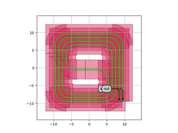
DoubleSpiralWithInCoupling
- class picazzo3.wg.spirals.cell.DoubleSpiralWithInCoupling
Double spiral class with both access waveguides on the outside of the spiral. In coupling waveguides are added to the spiral, one at the east side and one at the west side. The trace template provided in the property
trace_templateis used to build a chain of waveguides.- Parameters:
- n_o_loops: int and number > 0
Number of loops in the spiral
- trace_template: PCell and _TraceTemplate
Trace template used in the chain.
- name: String that contains only ISO/IEC 8859-1 (extended ASCII py3) or pure ASCII (py2) characters
The unique name of the pcell
- Other Parameters:
- n_o_traces: int and number > 0, locked
Total number of traces used in the spiral.
- traces: List with type restriction, allowed types: <class ‘ipkiss3.pcell.cell.pcell.PCell’>, locked
Views
- class Layout
- Parameters:
- incoupling_length: float and Real, number and number >= 0
length of the incoupling section.
- shapes: list
List of shapes used to build the traces
- flatten: ( bool, bool_ or int )
If true the instances are flattened
- inner_size: Coord2 and number >= 0
Inner size of the the spiral, defaults to 3 * spacing + 2 * bend_radius, in each direction
- view_name: String that contains only alphanumeric characters from the ASCII set or contains _$. ASCII set is extended on PY3.
The name of the view
- stub_direction: List with value restriction, allowed values: [‘H’, ‘V’]
- spacing: float and Real, number and number >= 0
spacing between the individual loops.
- Other Parameters:
- auto_transform: locked
- spiral_center: locked
Examples
import si_fab.all as pdk  # noqa: F401
from picazzo3.wg.spirals import DoubleSpiralWithInCoupling
from ipkiss3 import all as i3

cell = DoubleSpiralWithInCoupling(n_o_loops=3, trace_template=i3.TECH.PCELLS.WG.DEFAULT)
layout = cell.Layout(inner_size=(30.0, 30.0), incoupling_length=10.0, spacing=5)

layout.visualize(annotate=True)
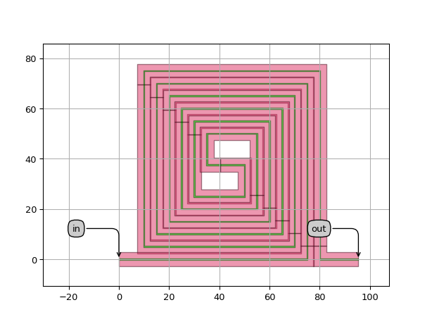
DoubleSpiralWithInCouplingRounded
- class picazzo3.wg.spirals.cell.DoubleSpiralWithInCouplingRounded
Rounded double spiral class with both access waveguides on the outside of the spiral. In coupling waveguides are added to the spiral, one at the east side and one at the west side. The trace template provided in the property
trace_templateis used to build a chain of waveguides. All the rounding properties can be set at the layout level.- Parameters:
- n_o_loops: int and number > 0
Number of loops in the spiral
- trace_template: PCell and _TraceTemplate
Trace template used in the chain.
- name: String that contains only ISO/IEC 8859-1 (extended ASCII py3) or pure ASCII (py2) characters
The unique name of the pcell
- Other Parameters:
- n_o_traces: int and number > 0, locked
Total number of traces used in the spiral.
- traces: List with type restriction, allowed types: <class ‘ipkiss3.pcell.cell.pcell.PCell’>, locked
Views
- class Layout
- Parameters:
- incoupling_length: float and Real, number and number >= 0
length of the incoupling section.
- shapes: list
List of shapes used to build the traces
- flatten: ( bool, bool_ or int )
If true the instances are flattened
- spacing: float and Real, number and number >= 0
spacing between the individual loops.
- stub_direction: List with value restriction, allowed values: [‘H’, ‘V’]
- inner_size: Coord2 and number >= 0
Inner size of the the spiral, defaults to 3 * spacing + 2 * bend_radius, in each direction
- view_name: String that contains only alphanumeric characters from the ASCII set or contains _$. ASCII set is extended on PY3.
The name of the view
- manhattan: ( bool, bool_ or int )
Adds rectangular blocks in the bends to avoid as much as possible non-manhattan angles.
- angle_step: float and number > 0
Angle step for rounding.
- rounding_algorithm:
Rounding algorithm used to generate the bends. Can be circular, spline, ….
- bend_radius: float and number > 0
Bend radius for the auto-generated bends.
- Other Parameters:
- auto_transform: locked
- spiral_center: locked
Examples
import si_fab.all as pdk  # noqa: F401
from picazzo3.wg.spirals import DoubleSpiralWithInCouplingRounded
from ipkiss3 import all as i3

cell = DoubleSpiralWithInCouplingRounded(n_o_loops=3, trace_template=i3.TECH.PCELLS.WG.DEFAULT)
layout = cell.Layout(
    inner_size=(30.0, 30.0), incoupling_length=10.0, bend_radius=3.0, manhattan=False, spacing=5.0
)

layout.visualize(annotate=True)
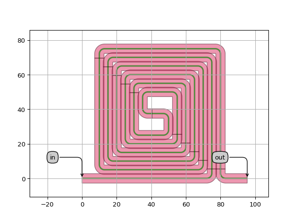
FixedLengthSpiral
- class picazzo3.wg.spirals.cell.FixedLengthSpiral
Spiral with incoupling sections that calculates its length. The total length is set by the property
total_lengthand the inner size of the spiral will be adapted so that the total length of the spiral (including the incoupling sections) would be equal tototal_length. The way this inner size is calculated can set using properties in the Layout view.- Parameters:
- total_length: float and number > 0
Total design length of the spiral.
- n_o_loops: int and number > 0
Number of loops in the spiral
- trace_template: PCell and _TraceTemplate
Trace template used in the chain.
- name: String that contains only ISO/IEC 8859-1 (extended ASCII py3) or pure ASCII (py2) characters
The unique name of the pcell
- Other Parameters:
- n_o_traces: int and number > 0, locked
Total number of traces used in the spiral.
- traces: List with type restriction, allowed types: <class ‘ipkiss3.pcell.cell.pcell.PCell’>, locked
Views
- class Layout
The inner size of the spiral is calculated by assuming a minimal inner_size and growing it in either the direction set by
growth_direction. An error is raised when that is impossible to do with the set number of loops.- Parameters:
- growth_direction: List with value restriction, allowed values: [‘H’, ‘V’]
- incoupling_length: float and Real, number and number >= 0
length of the incoupling section.
- shapes: list
List of shapes used to build the traces
- flatten: ( bool, bool_ or int )
If true the instances are flattened
- view_name: String that contains only alphanumeric characters from the ASCII set or contains _$. ASCII set is extended on PY3.
The name of the view
- stub_direction: List with value restriction, allowed values: [‘H’, ‘V’]
- spacing: float and Real, number and number >= 0
spacing between the individual loops.
- Other Parameters:
- auto_transform: locked
- inner_size: locked
- spiral_center: locked
Examples
import si_fab.all as pdk  # noqa: F401
from picazzo3.wg.spirals import FixedLengthSpiral
from ipkiss3 import all as i3

cell = FixedLengthSpiral(total_length=4000, n_o_loops=6, trace_template=i3.TECH.PCELLS.WG.DEFAULT)

layout = cell.Layout(
    incoupling_length=10.0,
    spacing=4,
    stub_direction="H",  # either H or V
    growth_direction="V",  # either H or V
)

# Checking if the trace length is indeed correct
print(layout.trace_length())

layout.visualize(annotate=True)
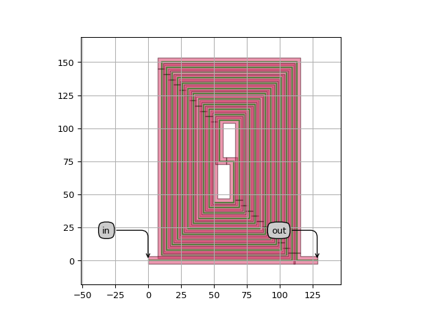
FixedLengthSpiralRounded
- class picazzo3.wg.spirals.cell.FixedLengthSpiralRounded
Rounded spiral with incoupling sections that calculates its length. The total length is set by the property
total_lengthand the inner size of the spiral will be adapted so that the total length of the spiral (including the incoupling sections) would be equal tototal_length. The way this inner size is calculated can set using properties in the Layout view.- Parameters:
- total_length: float and number > 0
Total design length of the spiral.
- n_o_loops: int and number > 0
Number of loops in the spiral
- trace_template: PCell and _TraceTemplate
Trace template used in the chain.
- name: String that contains only ISO/IEC 8859-1 (extended ASCII py3) or pure ASCII (py2) characters
The unique name of the pcell
- Other Parameters:
- n_o_traces: int and number > 0, locked
Total number of traces used in the spiral.
- traces: List with type restriction, allowed types: <class ‘ipkiss3.pcell.cell.pcell.PCell’>, locked
Views
- class Layout
The inner size of the spiral is calculated by assuming a minimal inner_size and growing it in either the direction set by
growth_direction. An error is raised when that is impossible to do with the set number of loops.- Parameters:
- growth_direction: List with value restriction, allowed values: [‘H’, ‘V’]
- incoupling_length: float and Real, number and number >= 0
length of the incoupling section.
- shapes: list
List of shapes used to build the traces
- flatten: ( bool, bool_ or int )
If true the instances are flattened
- spacing: float and Real, number and number >= 0
spacing between the individual loops.
- stub_direction: List with value restriction, allowed values: [‘H’, ‘V’]
- view_name: String that contains only alphanumeric characters from the ASCII set or contains _$. ASCII set is extended on PY3.
The name of the view
- manhattan: ( bool, bool_ or int )
Adds rectangular blocks in the bends to avoid as much as possible non-manhattan angles.
- angle_step: float and number > 0
Angle step for rounding.
- rounding_algorithm:
Rounding algorithm used to generate the bends. Can be circular, spline, ….
- bend_radius: float and number > 0
Bend radius for the auto-generated bends.
- Other Parameters:
- auto_transform: locked
- spiral_center: locked
- inner_size: locked
Examples
import si_fab.all as pdk  # noqa: F401
from picazzo3.wg.spirals import FixedLengthSpiralRounded
from ipkiss3 import all as i3

cell = FixedLengthSpiralRounded(total_length=4000, n_o_loops=6, trace_template=i3.TECH.PCELLS.WG.DEFAULT)

layout = cell.Layout(
    incoupling_length=10.0,
    bend_radius=10.0,
    spacing=4,
    stub_direction="H",  # either H or V
    growth_direction="V",  # either H or V
)

# Checking if the trace length is indeed correct
print(layout.trace_length())

layout.visualize(annotate=True)
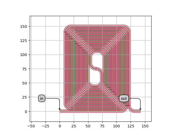
Placement and Routing
ConnectComponents
- class ipkiss3.pcell.container.connect_components.ConnectComponents
Parametric Cell for logically connecting multiple components.
The user supplies a dictionary of the instances of child cells that need to be placed through the property
child_cells. This dictionary maps the instance names to the PCell objects. The same PCell object can be used for multiple instances.child_cells={ "ring1" : my_ring1, "ring2" : my_ring2, "spl" : my_splitter, "com" : my_splitter # the same cell is used both for splitting and combining }
The connectivity between the instances of the child cells is set by a list of tuples containing pairs of instance terms/port names. This list
linksis of the forminstname:portnamelinks=[ ("spl:arm1", "arm1:in1"), ("arm1:out1", "com:arm1"), ("spl:arm2", "arm2:in1"), ("arm2:out1", "com:arm2") ]
All the terms of the instances are connected to outside terms. You can override the default external term names using the
external_port_namesproperty. There you can specify the individual names of the external terms. If no name is specified, the default pattern of ‘instname_termname’ will be used.external_port_names={ "spl:in1" : "input", "com:out1" : "output" }
- Parameters:
- links: list and List with type restriction, allowed types: [<class ‘collections.abc.Sequence’>]
list of tuples connecting the instances. Format is [(‘inst1:term1’,’inst2:term2’), …]
- external_port_names: str
Map of the free instance terms/ports to the names of external terms/ports.Format is a dict {‘inst:term’ : ‘new_term_name’}.If a term/port is not listed, the format instname_portname will be used
- child_cells:
dict to create the instances of the child cells.Format is {‘inst_name1’: PCell}
- name: String that contains only ISO/IEC 8859-1 (extended ASCII py3) or pure ASCII (py2) characters
The unique name of the pcell
Examples
"""Here we connect 2 splitters and two rings into a RLMZI
We use the splitter twice but use two different rings.
"""
import si_fab.all as pdk  # noqa: F401
from ipkiss3 import all as i3  # noqa: F401
import numpy as np
import pylab as plt

from picazzo3.filters.ring import RingRectNotchFilter
from picazzo3.wg.splitters import WgY90Splitter

ring1 = RingRectNotchFilter()
cp = {"cross_coupling1": 0.4j, "straight_coupling1": (1 - 0.4**2) ** 0.5}
ring1.CircuitModel(coupler_parameters=[cp], ring_length=50.0)

ring2 = RingRectNotchFilter()
ring2.CircuitModel(coupler_parameters=[cp], ring_length=55.0)

splitter = WgY90Splitter()

pc = i3.ConnectComponents(
    child_cells={"spl": splitter, "com": splitter, "arm1": ring1, "arm2": ring2},
    links=[
        ("spl:arm1", "arm1:in"),
        ("arm1:out", "com:arm1"),
        ("spl:arm2", "arm2:in"),
        ("arm2:out", "com:arm2"),
    ],
)

cm = pc.CircuitModel()

# Caphe simulation
wavelengths = np.linspace(1.50, 1.6, 2001)
R = cm.get_smatrix(wavelengths=wavelengths)

plt.plot(wavelengths, np.abs(R["spl_center", "com_center"]) ** 2, "b", label="power")
plt.title("Waveguide transmission (Power)")
plt.xlabel(r"Wavelength ($\mu m$)")
plt.ylabel("Power transmission")
plt.legend()
plt.show()
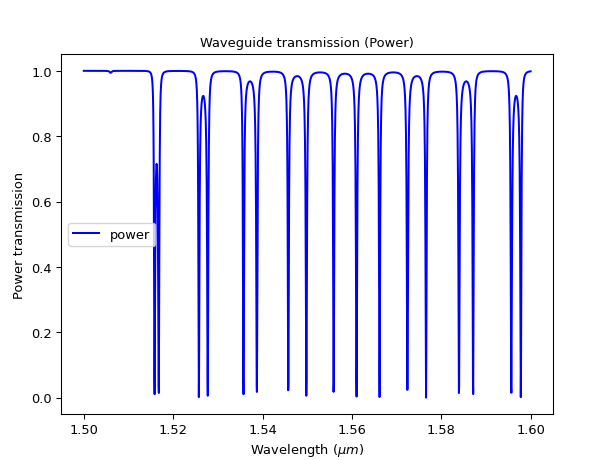
Views
- class Layout
- Parameters:
- view_name: String that contains only alphanumeric characters from the ASCII set or contains _$. ASCII set is extended on PY3.
The name of the view
PlaceAndConnect
- class picazzo3.routing.place_route.cell.PlaceAndConnect
Parametric Cell for manual placement and Logical connection of components.
The user supplies a dictionary of the instances of child cells that need to be placed through the property
child_cells. This dictionary maps the instance names to the PCell objects. The same PCell object can be used for multiple instances.child_cells={ "ring1" : my_ring1, "ring2" : my_ring2, "spl" : my_splitter, "com" : my_splitter # the same cell is used both for splitting and combining }
The connectivity between the instances of the child cells is set by a list of tuples containing pairs of instance terms/port names. This list
linksis of the forminstname:portnamelinks=[ ("spl:arm1", "arm1:in1"), ("arm1:out1", "com:arm1"), ("spl:arm2", "arm2:in1"), ("arm2:out1", "com:arm2") ]
All the unused terms of the instances are connected to outside terms. You can override the default external term names using the
external_port_namesproperty. There you can specify the individual names of the external terms. If no name is specified, the default pattern of ‘instname_termname’ will be used.external_port_names={ "spl:in1" : "input", "com:out1" : "output" }
The PCell will place the waveguides and connect them logically in the netlist, but it is up to the user to verify whether the physical location of the connected ports matches.
In the layout, the placement is specified manually using the
child_transformationsproperty, which defines a transformation for each instance. If no transformation is supplied for an instance, no transformation will be applied. It is also possible to supply a coordinate (Coord2) or tuple, which will be interpreted as a position for placement.child_transformations={"arm1": (50, -50), "arm2": (50,50), "com": i3.HMirror(0.0)+i3.Translation((100,0))}
Child cells that are logically connected but where the ports are not physically connected (e.g. by wrong placement), will be connected with visual flylines.
You can subclass this PCell in order to implement your own additional functionality, or define subcircuits that define their own child cells and child transformations. Warning: do not refer to self.child_cells from within an overridden _default_child_transformations - rather refer to the child cell directly (like self.my_child_cell).
- Parameters:
- links: list and List with type restriction, allowed types: [<class ‘collections.abc.Sequence’>]
list of tuples connecting the instances. Format is [(‘inst1:term1’,’inst2:term2’), …]
- external_port_names: str
Map of the free instance terms/ports to the names of external terms/ports.Format is a dict {‘inst:term’ : ‘new_term_name’}.If a term/port is not listed, the format instname_portname will be used
- child_cells:
dict to create the instances of the child cells. Format is {‘inst_name1’: PCell}
- name: String that contains only ISO/IEC 8859-1 (extended ASCII py3) or pure ASCII (py2) characters
The unique name of the pcell
Views
- class Layout
- Parameters:
- flyline_width: float and number > 0
line width of the flylines
- flyline_layer: ( __Layer__ ), *None allowed*
layer to draw flylines of physically unconnected links
- child_transformations:
dictionary with the transformation of each child instance.
- netlist_view: NetlistView
Netlist view in the same cell on which this Layout is based. Normally no need to manually override.
- view_name: String that contains only alphanumeric characters from the ASCII set or contains _$. ASCII set is extended on PY3.
The name of the view
Examples
"""Here we connect together 2 splitters and two rings to form a Ring-loaded
Mach-Zehnder. We use the splitter twice (as splitter and combiner) but use
two different rings. We calculate the transformations of the rings in such
a way that they attach correctly to the splitter and combiner
"""
import si_fab.all as pdk  # noqa: F401
from ipkiss3 import all as i3  # noqa: F401

from picazzo3.filters.ring import RingRect180DropFilter, RingRectNotchFilter
from picazzo3.wg.splitters import WgY180Splitter

from picazzo3.routing.place_route import PlaceAndConnect

from ipkiss.geometry.vector import vector_match_transform

# both rings have the same size
ring1 = RingRectNotchFilter()
ring1_layout = ring1.Layout()
ring2 = RingRect180DropFilter()
ring2_layout = ring2.Layout()
splitter = WgY180Splitter()
splitter_layout = splitter.Layout()

pr = PlaceAndConnect(
    child_cells={
        "spl": splitter,
        "com": splitter,
        "arm1": ring1,
        "arm2": ring2,
    },
    links=[
        ("spl:arm1", "arm1:in"),
        ("arm1:out", "com:arm1"),
        ("spl:arm2", "arm2:in1"),
        ("arm2:out1", "com:arm2"),
    ],
)

# manually calculate the transformations needed to attach the ports together
t_ring1 = vector_match_transform(ring1_layout.ports["in"], splitter_layout.ports["arm1"])
t_ring2 = vector_match_transform(ring2_layout.ports["in1"], splitter_layout.ports["arm2"])
t_com = (
    vector_match_transform(splitter_layout.ports["arm1"], ring1_layout.ports["out"], mirrored=True)
    + t_ring1
)

layout = pr.Layout(child_transformations={"arm1": t_ring1, "arm2": t_ring2, "com": t_com})
layout.visualize(annotate=True)
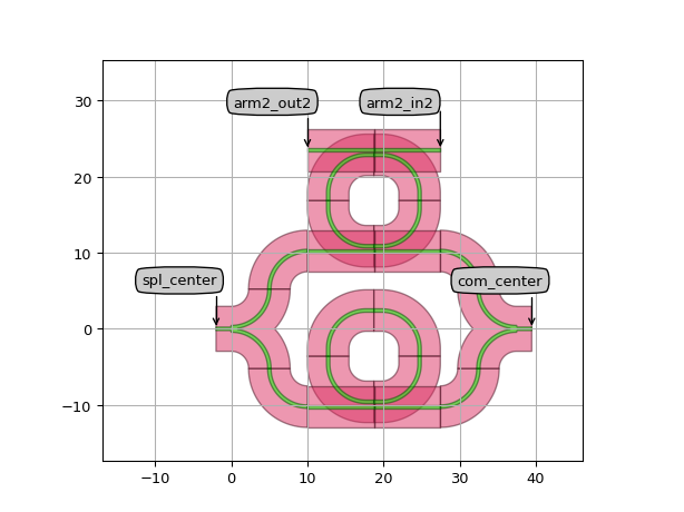
Apertures
OpenAperture
- class picazzo3.apertures.basic.cell.OpenAperture
Abstract base class for apertures into a slab area
- Parameters:
- aperture_trace_template: PCell and _TraceTemplate
template of the aperture cross-section
- trace_template: PCell and _TraceTemplate
template of the start waveguide
- name: String that contains only ISO/IEC 8859-1 (extended ASCII py3) or pure ASCII (py2) characters
The unique name of the pcell
Views
- class Layout
- Parameters:
- transition_length: float and number > 0
transition length
- center: Coord2
center coordinate
- view_name: String that contains only alphanumeric characters from the ASCII set or contains _$. ASCII set is extended on PY3.
The name of the view
WireWgAperture
- class picazzo3.apertures.basic.cell.WireWgAperture
Wire waveguide aperture into a slab area
- Parameters:
- aperture_trace_template: PCell and _TraceTemplate
template of the aperture cross-section
- trace_template: PCell and _TraceTemplate
template of the start waveguide
- name: String that contains only ISO/IEC 8859-1 (extended ASCII py3) or pure ASCII (py2) characters
The unique name of the pcell
Views
- class Layout
- Parameters:
- aperture_trench_width: float and Real, number and number >= 0
Width of the cladding/trench extending from the core at the aperture side. Defaults to that of aperture_trace_template
- trench_width: float and Real, number and number >= 0
Width of the cladding/trench extending from the core at the input side. Defaults to that of trace_template
- transition_length: float and number > 0
transition length
- center: Coord2
center coordinate
- view_name: String that contains only alphanumeric characters from the ASCII set or contains _$. ASCII set is extended on PY3.
The name of the view
Examples
import si_fab.all as pdk  # noqa: F401
from ipkiss3 import all as i3
from picazzo3.apertures.basic import WireWgAperture
from picazzo3.traces.wire_wg import WireWaveguideTemplate

wt = WireWaveguideTemplate()
wt.Layout(core_width=0.9, cladding_width=2 * i3.TECH.WG.WIRE_WIDTH + 0.9)
wwa = WireWgAperture(aperture_trace_template=wt)
wwa_lay = wwa.Layout()
wwa_lay.visualize(annotate=True)
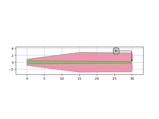
Containers and adapters
AutoTransitionPorts
AutoTransitionPorts
- class picazzo3.container.transition_ports.AutoTransitionPorts
Pcell containing another PCell with transitions on all (labeled) ports, using AutoTraceTransitionFromPort. The target trace template is defined in
trace_template.- Parameters:
- trace_template: ( PCell and _WaveguideTemplate ), *None allowed*
Template for all ports, defaults to TECH.PCELLS.WG.DEFAULT.When set to None, the waveguide templates of the ports will be used.
- transition_database: AutoTransitionDatabase
AutoTransitionDatabase in which the correct transition between the two trace templates can be looked up.
- transitions: List with type restriction, allowed types: <class ‘ipkiss3.pcell.cell.pcell.PCell’>
Transitions (of type WaveguideTransitionFromPort) attached the the ports given in port_labels. Should be in the same order as port_labels.
- port_labels: ( List with type restriction, allowed types: <class ‘str’> ), *None allowed*
Labels of the ports to be processed. Set to None to process all ports.
- external_port_names: str
Dictionary for remapping of the port names of the contents to the external ports
- contents: PCell
the contents of the container: the child cell
- name: String that contains only ISO/IEC 8859-1 (extended ASCII py3) or pure ASCII (py2) characters
The unique name of the pcell
- Other Parameters:
- trace_templates: List with type restriction, allowed types: <class ‘ipkiss3.pcell.cell.pcell.PCell’>, locked
list of templates to apply to all ports
Examples
Tapering ports to a wider width:
import si_fab.all as pdk  # noqa: F401
from picazzo3.filters.ring import RingRect180DropFilter
from picazzo3.traces.wire_wg import WireWaveguideTemplate

my_ring = RingRect180DropFilter()
my_ring.Layout()
from picazzo3.container.transition_ports import AutoTransitionPorts

wire_t = WireWaveguideTemplate()
wire_t.Layout(core_width=0.7, cladding_width=0.7 + 2 * 2.0)
my_ring_tapered_auto = AutoTransitionPorts(
    contents=my_ring, port_labels=["W0", "W1", "E0"], trace_template=wire_t
)
my_ring_tapered_auto_layout = my_ring_tapered_auto.Layout()
my_ring_tapered_auto_layout.visualize(annotate=True)
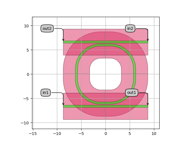
Using _transition_parameters:
import si_fab.all as pdk  # noqa: F401
from picazzo3.traces.rib_wg import RibWaveguideTemplate
from picazzo3.traces.wire_wg import WireWaveguideTemplate
from picazzo3.container.transition_ports import AutoTransitionPorts
import ipkiss3.all as i3

class MyCell(i3.PCell):
    class Layout(i3.LayoutView):
        def _generate_elements(self, elems):
            elems += i3.Circle(layer=i3.TECH.PPLAYER.SI)
            return elems

        def _generate_ports(self, ports):
            ports += i3.OpticalPort(name="in", position=(5.0, 0.0), trace_template=RibWaveguideTemplate())
            ports += i3.OpticalPort(
                name="out", position=(-5.0, 0.0), angle=180, trace_template=RibWaveguideTemplate()
            )
            return ports

trace_template = WireWaveguideTemplate()
auto_transition_ports = AutoTransitionPorts(
    contents=MyCell(),
    trace_template=trace_template,
)
auto_transition_ports_lv = auto_transition_ports.Layout(_transition_parameters={"length": 5.0})
auto_transition_ports_lv.visualize(annotate=True)
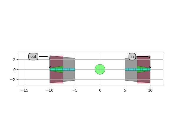
Views
- class Layout
- Parameters:
- transition_length: ( float and Real, number and number >= 0 ), *None allowed*
Length of the transition. Set to None to take the standard transition length.
- zero_length_if_identical: ( bool, bool_ or int )
uses a zero-length transition if the trace templates are identical
- flatten_transitions: ( bool, bool_ or int )
if true, flattens the transitions one level
- straight_extension: ( Coord2 and number >= 0 ), *None allowed*
Tuple: straight extensions of the transitions. Set to None to take the standard straight extensions
- contents_transformation: GenericNoDistortTransform
transformation to apply to the contents
- flatten_contents: ( bool, bool_ or int )
if True, it will insert the contents as elements in the layout, rather than as an Instance
- view_name: String that contains only alphanumeric characters from the ASCII set or contains _$. ASCII set is extended on PY3.
The name of the view
- Other Parameters:
- transition_lengths: locked
FanoutPorts
FanoutPorts
- class picazzo3.container.fanout_ports.FanoutPorts
Fanout Container. Routes all ports listed in
port_labelsinto a given direction, with a given spacing. This is typically used to redirect a set of ports on a component to a regularly spaced array of ports. The user can use this to convert from one input/output waveguide pitch to another, or from irregular input/output waveguide positioning to a regular pitch.If
port_labelsis not specified, all ports will be routed.By default, the default waveguide template specified in the technology, TECH.PCELLS.WG.DEFAULT, will be used. This can be overridden by setting trace_template=None, in which case the trace templates of the ports of the contents will be used.
- Parameters:
- trace_template: ( PCell and _WaveguideTemplate ), *None allowed*
Template for all ports, defaults to TECH.PCELLS.WG.DEFAULT.When set to None, the waveguide templates of the ports will be used.
- auto_transition: ( bool, bool_ or int )
If True, automatically transition all ports of contents to the given trace template. If False, no transitions are applied, which might lead to a discontinuity in the waveguide. Also, if trace_template is None, no transitions are applied.
- port_labels: ( List with type restriction, allowed types: <class ‘str’> ), *None allowed*
Labels of the ports to be processed. Set to None to process all ports.
- external_port_names: str
Dictionary for remapping of the port names of the contents to the external ports
- contents: PCell
the contents of the container: the child cell
- name: String that contains only ISO/IEC 8859-1 (extended ASCII py3) or pure ASCII (py2) characters
The unique name of the pcell
- Other Parameters:
- bundle: ( PCell ), locked, *None allowed*
bundle of waveguides added to the contents, generated based on the supplied waveguides list
- waveguides: List with type restriction, allowed types: <class ‘ipkiss3.pcell.cell.pcell.PCell’>, locked
- trace_templates: List with type restriction, allowed types: <class ‘ipkiss3.pcell.cell.pcell.PCell’>, locked
list of templates to apply to all ports
Views
- class Layout
- Parameters:
- target_coordinate: ( float ), *None allowed*
The coordinate where the endpoints of the waveguides are aligned. An x-coordinate when routing toEAST or WEST, a y-coordinate when routing to NORTH or SOUTH. When the waveguides extend beyond thetarget coordinate, the value is ignored.
- max_s_bend_angle: float and ]0.0,90.0]
- spacing: float
spacing between adjacent output waveguides
- align_outputs: ( bool, bool_ or int )
If True, all outputs will be aligned to the outermost waveguide end, even if it extends beyond its target coordinate.
- reference_coordinate: ( float ), *None allowed*
The coordinate where the first waveguide will be aligned. An x-coordinate if routed towards NORTH or SOUTH,a y-coordinate when routed towards EAST or WEST. If not specified, the x or y coordinate of the first port is taken.
- output_direction: List with value restriction, allowed values: [C2(1.000000, 0.000000), C2(-1.000000, 0.000000), C2(0.000000, 1.000000), C2(0.000000, -1.000000)]
direction of the output waveguides. Should be EAST, WEST, NORTH or SOUTH
- area_layer_on: ( bool, bool_ or int )
When True, the waveguide area will be covered by i3.Rectangles on all cover layers.
- routes:
routes along which the waveguides will be generated
- contents_transformation: GenericNoDistortTransform
transformation to apply to the contents
- flatten_contents: ( bool, bool_ or int )
if True, it will insert the contents as elements in the layout, rather than as an Instance
- view_name: String that contains only alphanumeric characters from the ASCII set or contains _$. ASCII set is extended on PY3.
The name of the view
- manhattan: ( bool, bool_ or int )
Adds rectangular blocks in the bends to avoid as much as possible non-manhattan angles.
- angle_step: float and number > 0
Angle step for rounding.
- rounding_algorithm:
Rounding algorithm used to generate the bends. Can be circular, spline, ….
- bend_radius: float and number > 0
Bend radius for the auto-generated bends.
- Other Parameters:
- target_coordinates: locked
- max_s_bend_angles: locked
- spacings_from_reference: locked
Examples
import si_fab.all as pdk  # noqa: F401
from picazzo3.filters.ring import RingRect180DropFilter
from picazzo3.container.fanout_ports import FanoutPorts
from ipkiss3 import all as i3

my_ring = RingRect180DropFilter()
my_ring.Layout()

my_ring_fanout = FanoutPorts(contents=my_ring, port_labels=["E0", "E1"])

lay = my_ring_fanout.Layout(
    contents_transformation=i3.Rotation(rotation=10.0),
    flatten_contents=False,
    area_layer_on=False,  # if True, adds area layer on the bundle
    output_direction=i3.EAST,
    spacing=20.0,  # spacing between outputs
    reference_coordinate=-12.5,  # y-coordinate (or x for NORTH and SOUTH) of first waveguide
    target_coordinate=20.0,  # x-coordinate (or y for NORTH and SOUTH) of output port
    max_s_bend_angle=45.0,  # maximum angle of S-bend
    bend_radius=4.5,  # bend radius of waveguides
)
lay.visualize(annotate=True)
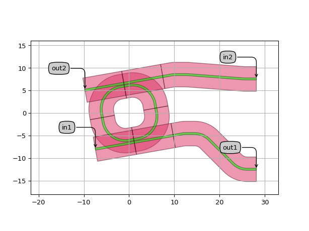
import si_fab.all as pdk  # noqa: F401
from picazzo3.filters.ring import RingRect180DropFilter
from picazzo3.traces.wire_wg import WireWaveguideTemplate
from picazzo3.container.fanout_ports import FanoutPorts
from ipkiss3 import all as i3

wg_t1 = WireWaveguideTemplate()
wg_t1.Layout(core_width=0.55)
wg_t2 = WireWaveguideTemplate()
wg_t2.Layout(core_width=0.35)

my_ring = RingRect180DropFilter(name="ring_for_fanout", coupler_trace_templates=[wg_t1, wg_t2])
my_ring.Layout()

my_ring_fanout = FanoutPorts(
    contents=my_ring,
    port_labels=["E0", "E1"],
    trace_template=wg_t1,
    auto_transition=True,  # this adds transitions when the waveguide templates don't match.
)

layout = my_ring_fanout.Layout(
    contents_transformation=i3.Rotation(rotation=10.0),
    flatten_contents=False,
    area_layer_on=False,  # draws a cover layer between the waveguides
    output_direction=i3.DIRECTION.EAST,
    spacing=20.0,  # spacing between outputs
    max_s_bend_angle=60.0,  # maximum angle of S-bend
    bend_radius=10.0,  # bend radius of waveguides
)
layout.visualize(annotate=True)
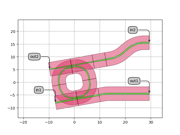
IoFibcoup
IoFibcoupGeneric
- class picazzo3.container.iofibcoup.IoFibcoupGeneric
generic adapter for grating fiber couplers.
The component East and West ports are treated separately, and routed towards the East and West, respectively. For this routing, they go through several steps.
Here, we discuss the use for the East ports, but a similar set of parameters is available for the West ports. A lot of the properties are “plural”. This means that they can accept a list of parameters (e.g.
east_trace_templates). This allows you to specify the template (or other parameter) for each individual port. The lists do not need to have the exact same length as the number of ports. If the number of elements is different from the number of ports in your component, theIoFibcoupGenericwill just cycle through the list. That way, if all the ports use the same value, you only need to supply a list of one element.First of all, the ports of the component are transitioned to a common trace template
east_trace_templates. By default, it uses the standard waveguide definition defined inTECH.PCELLS.WG.DEFAULT. However, if an element of the list isNone, it will use the trace template of the actual port. The same holds foreast_transition_lengths. This can be manually specified by the user, but if a value in the list is set toNone, the default length of that transition will be used.Then, the ports are fanned out to the fixed
y_spacingof the fiber couplers. The length of that Fanout can be specified througheast_fanout_length. Bend radius and rounding algorithm is shared between all ports in the parameterbend_radiusandrounding_algorithm. Ifwest_bundle_tracesisTrue, the cover layers will be drawn over the Fanout. This can help reduce DRC errors.Then, the waveguides are transitioned to another waveguide template, specified in
east_connect_trace_templates. By default, this is the same template aseast_trace_templates, but it is possible to override it to use a lower loss multi-mode waveguide. The connection for which this waveguide is used is a simple straight connection, but depending on the chip layout it can have a long length. The transition lengths can be manually specified using theeast_connect_transition_lengths.At the output, the waveguides are transitioned to the waveguide template of the individual input and output fiber couplers. The transition lengths from the connection waveguide to the grating coupler can be specified using
east_fiber_coupler_transition_lengths.Finally, the circuit is terminated with the individual fiber couplers, specified in
east_fiber_couplers
The same procedure and parameters are used for the west ports
- Parameters:
- west_trace_templates: List with type restriction, allowed types: <class ‘ipkiss3.pcell.cell.pcell.PCell’> and ( _WaveguideTemplate or None ) and [1,inf]
The trace templates that will be used for the Fanout of the West ports. and the traces of the Fanout. If an entry of the list is ‘None’, the trace template of the individual port will be used. Defaults to
[TECH.PCELLS.WG.DEFAULT]. The number of entries in the list should not be identical to the number of West port. If the component has fewer West ports, only the first entries in the list will be used. If the component has more West ports, the list is just recycled. Therefore, it is allowed to use a list of just one element for multiple ports.- east_trace_templates: List with type restriction, allowed types: <class ‘ipkiss3.pcell.cell.pcell.PCell’> and ( _WaveguideTemplate or None ) and [1,inf]
The trace templates that will be used for the Fanout of the East ports. and the traces of the Fanout. If an entry of the list is ‘None’, the trace template of the individual port will be used. Defaults to
[TECH.PCELLS.WG.DEFAULT]. The number of entries in the list should not be identical to the number of East port. If the component has fewer East ports, only the first entries in the list will be used. If the component has more East ports, the list is just recycled. Therefore, it is allowed to use a list of just one element for multiple ports.- west_connect_trace_templates: List with type restriction, allowed types: <class ‘ipkiss3.pcell.cell.pcell.PCell’> and ( _WaveguideTemplate or None ) and [1,inf]
The trace templates that will be used for connecting the Fanout of the West ports. to the Grating couplers. If an entry of the list is ‘None’, the trace template of the individual port will be used. Defaults to the same as
west_trace_templates. The number of entries in the list should not be identical to the number of West port. If the component has fewer West ports, only the first entries in the list will be used. If the component has more West ports, the list is just recycled. Therefore, it is allowed to use a list of just one element for multiple ports.- east_connect_trace_templates: List with type restriction, allowed types: <class ‘ipkiss3.pcell.cell.pcell.PCell’> and ( _WaveguideTemplate or None ) and [1,inf]
The trace templates that will be used for connecting the Fanout of the East ports. to the Grating couplers. If an entry of the list is ‘None’, the trace template of the individual port will be used. Defaults to the same as
east_trace_templates. The number of entries in the list should not be identical to the number of East port. If the component has fewer East ports, only the first entries in the list will be used. If the component has more East ports, the list is just recycled. Therefore, it is allowed to use a list of just one element for multiple ports.- west_fiber_coupler_external_port_name_maps: str
list of dicts to map the names of the West fiber coupler ports that will be exposed as external ports. The format is [dict1, dict2, …] with for each termination a dict of the form {‘port_name_on_termination’: ‘unique_external_port_name’, …}. the ‘unique_external_port_name’ string can contain the identifier {port}, which will be replaced by the corresponding port name on the component.The number of entries in the list should not be identical to the number of West port. If the component has fewer West ports, only the first entries in the list will be used. If the component has more West ports, the list is just recycled. Therefore, it is allowed to use a list of just one element for multiple ports. For example, the default is [{‘vertical_in’ : ‘{port}’}], which will map the port ‘vertical_in’ of the fiber coupler to the name of port on the component.
- west_fiber_coupler_port_labels: List with type restriction, allowed types: <class ‘str’>
Port labels of the West fiber couplers connected to the ports of the contents. For fiber couplers with more than one port, the port labels should be concatenated with a ‘,’. For example, when using 2D grating couplers, the ports could be [‘in1,in2’, ‘in’]. This will use ports ‘in1’ and ‘in2’ of the first grating coupler, and ‘in’ of the second.By default, all the East ports of the fiber coupler are used. If an entry in the list is ‘None’, also the East ports of that fiber coupler are used. The number of entries in the list should not be identical to the number of West port. If the component has fewer West ports, only the first entries in the list will be used. If the component has more West ports, the list is just recycled. Therefore, it is allowed to use a list of just one element for multiple ports.
- west_fiber_couplers: List with type restriction, allowed types: <class ‘ipkiss3.pcell.cell.pcell.PCell’> and [1,inf]
List of the fiber couplers to be attached on the West ports. Defaults to
[TECH.IO.FIBCOUP.DEFAULT.PCELLS.DEFAULT_GRATING]The number of entries in the list should not be identical to the number of West port. If the component has fewer West ports, only the first entries in the list will be used. If the component has more West ports, the list is just recycled. Therefore, it is allowed to use a list of just one element for multiple ports.- east_fiber_coupler_external_port_name_maps: str
list of dicts to map the names of the East fiber coupler ports that will be exposed as external ports. The format is [dict1, dict2, …] with for each termination a dict of the form {‘port_name_on_termination’: ‘unique_external_port_name’, …}. the ‘unique_external_port_name’ string can contain the identifier {port}, which will be replaced by the corresponding port name on the component.The number of entries in the list should not be identical to the number of East port. If the component has fewer East ports, only the first entries in the list will be used. If the component has more East ports, the list is just recycled. Therefore, it is allowed to use a list of just one element for multiple ports. For example, the default is [{‘vertical_in’ : ‘{port}’}], which will map the port ‘vertical_in’ of the fiber coupler to the name of port on the component.
- east_fiber_coupler_port_labels: List with type restriction, allowed types: <class ‘str’>
Port labels of the East fiber couplers connected to the ports of the contents. For fiber couplers with more than one port, the port labels should be concatenated with a ‘,’. For example, when using 2D grating couplers, the ports could be [‘in1,in2’, ‘in’]. This will use ports ‘in1’ and ‘in2’ of the first grating coupler, and ‘in’ of the second.By default, all the West ports of all the fiber couplers are used. If an entry in the list is ‘None’, also the west ports of that fiber coupler are used. The number of entries in the list should not be identical to the number of East port. If the component has fewer East ports, only the first entries in the list will be used. If the component has more East ports, the list is just recycled. Therefore, it is allowed to use a list of just one element for multiple ports.
- east_fiber_couplers: List with type restriction, allowed types: <class ‘ipkiss3.pcell.cell.pcell.PCell’> and [1,inf]
List of the fiber couplers to be attached on the East ports. Defaults to
[TECH.IO.FIBCOUP.DEFAULT.PCELLS.DEFAULT_GRATING]The number of entries in the list should not be identical to the number of East port. If the component has fewer East ports, only the first entries in the list will be used. If the component has more East ports, the list is just recycled. Therefore, it is allowed to use a list of just one element for multiple ports.- west_port_labels: ( List with type restriction, allowed types: <class ‘str’> ), *None allowed*
Labels of the ports to directed to the West. Set to None to process all West ports.
- east_port_labels: ( List with type restriction, allowed types: <class ‘str’> ), *None allowed*
Labels of the ports to directed to the East. Set to None to process all East ports.
- external_port_names: str
Dictionary for remapping of the port names of the contents to the external ports
- contents: PCell
the contents of the container: the child cell
- name: String that contains only ISO/IEC 8859-1 (extended ASCII py3) or pure ASCII (py2) characters
The unique name of the pcell
- Other Parameters:
- port_labels: locked
Examples
"""This example illustrates how the IoFibcoupGeneric properties can customize the routing in an IoColumn."""
import si_fab.all as pdk  # noqa: F401
from ipkiss3 import all as i3
from picazzo3.filters.mmi import MMIIdentical
from picazzo3.traces.wire_wg import WireWaveguideTemplate

wg_t1 = WireWaveguideTemplate()
wg_t1.Layout(core_width=7.0, cladding_width=8.0)
my_mmi = MMIIdentical(mmi_trace_template=wg_t1, n_inputs=1, n_outputs=5)
my_mmi.Layout(length=10.0, input_y_positions=[-1.0], output_y_positions=[-2.0, -1.0, 0.0, 1.0, 2.0])

from picazzo3.container.iofibcoup import IoFibcoupGeneric

from ipkiss3.pcell.blocks.iocolumn import IoColumn

my_column = IoColumn(name="iocol", adapter=IoFibcoupGeneric, max_n_o_lines=100)
my_column.Layout(south_east=(1500.0, 0.0))

my_column.add(my_mmi)
my_column.add(my_mmi, relative_offset=(0.0, 50.0), transformation=i3.Rotation(rotation=180.0))

my_column.Layout()
Views
- class Layout
- Parameters:
- west_fiber_coupler_transition_lengths: ( number >= 0 or None ) and [1,inf]
The lengths of the transitions between the West straight connection traces and the fiber coupler. If an entry of the list is ‘None’, the default length of the transition of that type will be used. Defaults to [None]. The number of entries in the list should not be identical to the number of West port. If the component has fewer West ports, only the first entries in the list will be used. If the component has more West ports, the list is just recycled. Therefore, it is allowed to use a list of just one element for multiple ports.
- east_fiber_coupler_transition_lengths: ( number >= 0 or None ) and [1,inf]
The lengths of the transitions between the East straight connection traces and the fiber coupler. If an entry of the list is ‘None’, the default length of the transition of that type will be used. Defaults to [None]. The number of entries in the list should not be identical to the number of East port. If the component has fewer East ports, only the first entries in the list will be used. If the component has more East ports, the list is just recycled. Therefore, it is allowed to use a list of just one element for multiple ports.
- west_connect_transition_lengths: ( number >= 0 or None ) and [1,inf]
The lengths of the transitions between the West fanout ports and the straight connection traces to the fiber coupler. If an entry of the list is ‘None’, the default length of the transition of that type will be used. Defaults to [None]. The number of entries in the list should not be identical to the number of West port. If the component has fewer West ports, only the first entries in the list will be used. If the component has more West ports, the list is just recycled. Therefore, it is allowed to use a list of just one element for multiple ports.
- east_connect_transition_lengths: ( number >= 0 or None ) and [1,inf]
The lengths of the transitions between the East fanout ports and the straight connection traces to the fiber coupler. If an entry of the list is ‘None’, the default length of the transition of that type will be used. Defaults to [None]. The number of entries in the list should not be identical to the number of East port. If the component has fewer East ports, only the first entries in the list will be used. If the component has more East ports, the list is just recycled. Therefore, it is allowed to use a list of just one element for multiple ports.
- west_transition_lengths: ( number >= 0 or None ) and [1,inf]
The lengths of the transitions between the West ports of the component and the traces of the Fanout. If an entry of the list is ‘None’, the default length of the transition of that type will be used. Defaults to [None]. The number of entries in the list should not be identical to the number of West port. If the component has fewer West ports, only the first entries in the list will be used. If the component has more West ports, the list is just recycled. Therefore, it is allowed to use a list of just one element for multiple ports.
- east_transition_lengths: ( number >= 0 or None ) and [1,inf]
The lengths of the transitions between the East ports of the component and the traces of the Fanout. If an entry of the list is ‘None’, the default length of the transition of that type will be used. Defaults to [None]. The number of entries in the list should not be identical to the number of East port. If the component has fewer East ports, only the first entries in the list will be used. If the component has more East ports, the list is just recycled. Therefore, it is allowed to use a list of just one element for multiple ports.
- west_max_s_bend_angles: ]0.0,90.0]
Maximum angle for the S-bend in the fanout of the West ports.
- east_max_s_bend_angles: ]0.0,90.0]
Maximum angles for the S-bend in the fanout of the East ports.
- west_bundle_traces: ( bool, bool_ or int )
Combine the Fanout waveguides on the West in a bundle (adding Cover layers)?
- west_align_fanout: ( bool, bool_ or int )
if True, the outputs of the waveguides in the West Fanout will be aligned.
- west_fanout_lengths: ( number > 0 or None )
Lengths of the waveguides in the Fanout section of the West ports. If an entry in the list is None the lengths will be chosen automatically.If the required length is larger than the specified length, additional space will be used.
- east_align_fanout: ( bool, bool_ or int )
if True, the outputs of the waveguides in the East Fanout will be aligned.
- east_bundle_traces: ( bool, bool_ or int )
Combine the Fanout waveguides on the east in a bundle (adding Cover layers)?
- east_fanout_lengths: ( number > 0 or None )
Lengths of the waveguides in the Fanout section of the East ports. If an entry in the list is None the lengths will be chosen automatically.If the required length is larger than the specified length, additional space will be used.
- west_fiber_coupler_transformations: List with type restriction, allowed types: <class ‘ipkiss.geometry.transforms.no_distort.NoDistortTransform’>
Transformations of the individual West fiber couplers, relative to the y_spacing grid of the adapter. By default, a no transformation is applied. The number of entries in the list should not be identical to the number of West port. If the component has fewer West ports, only the first entries in the list will be used. If the component has more West ports, the list is just recycled. Therefore, it is allowed to use a list of just one element for multiple ports.
- east_fiber_coupler_transformations: List with type restriction, allowed types: <class ‘ipkiss.geometry.transforms.no_distort.NoDistortTransform’>
Transformations of the individual East fiber couplers, relative to the y_spacing grid of the adapter. By default, a Horizontal Mirroring is applied. The number of entries in the list should not be identical to the number of East port. If the component has fewer East ports, only the first entries in the list will be used. If the component has more East ports, the list is just recycled. Therefore, it is allowed to use a list of just one element for multiple ports.
- relative_offset: Coord2
Offset of the component as it is positioned by absolute_offset
- absolute_offset: Coord2
Offset of the component from the (0,0) of the adapter.By default this offset will be calculated such that the component ports areX-aligned around the center and that the first West port is Y-aligned to the south_west.This is after the
contents_transformationhas been applied.- contents_transformation: GenericNoDistortTransform
transformation to apply to the contents
- flatten_contents: ( bool, bool_ or int )
if True, it will insert the contents as elements in the layout, rather than as an Instance
- outline_layer: __Layer__
Layer on which to draw the block outline
- draw_block_outline: ( bool, bool_ or int )
Draw the outline of the block when set to True
- south_east: Coord2
Position of the south east corner of the block
- south_west: Coord2
Position of the south west corner of the block
- y_spacing: float and number > 0
The spacing between blocks
- view_name: String that contains only alphanumeric characters from the ASCII set or contains _$. ASCII set is extended on PY3.
The name of the view
- manhattan: ( bool, bool_ or int )
Adds rectangular blocks in the bends to avoid as much as possible non-manhattan angles.
- angle_step: float and number > 0
Angle step for rounding.
- rounding_algorithm:
Rounding algorithm used to generate the bends. Can be circular, spline, ….
- bend_radius: float and number > 0
Bend radius for the auto-generated bends.
- Other Parameters:
- south_offset: int, locked
The y-offset between south_west & south_east, measured in units of y_spacing
- width: float and Real, number and number >= 0, locked
The width of the block, calculated using south_west & south_east
Examples
"""This example illustrates the default settings of IoFibcoupGeneric,
by adding a Ring resonator to the adapter"""
import si_fab.all as pdk  # noqa: F401
from picazzo3.filters.ring import RingRect180DropFilter

my_ring = RingRect180DropFilter()

from picazzo3.container.iofibcoup import IoFibcoupGeneric

iofb = IoFibcoupGeneric(contents=my_ring)
iofb_layout = iofb.Layout()
iofb_layout.visualize(annotate=True)
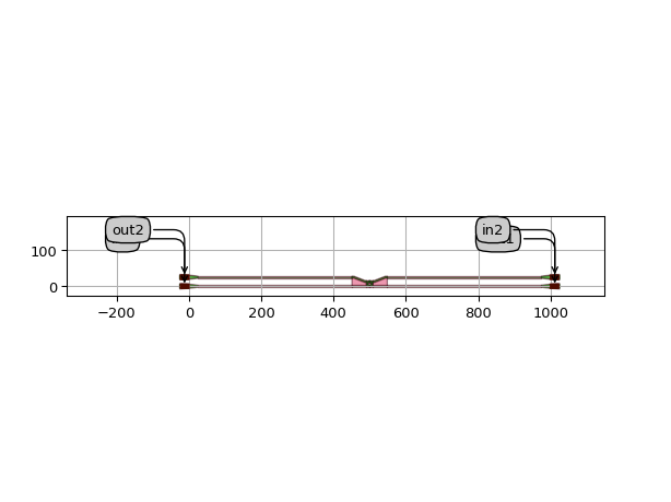
"""This example takes an MMI and encapsulates it in an IoFibcoup adapter.
It customizes several parameters of the adapter for individual tailoring of each input and output.
For instance, it explicitly lists the east ports of the MMI, skipping port 'out4'.
It also uses 2 different grating couplers on the East side, and 3 different transformations.
The cycling of the parameters will cause the fiber couplers to be repeated every even and odd line
(because there are 2 fiber couplers specified), while the transformation will repeat every 3 lines.
As a result, the 4 outputs of the MMI all have a different combination of fiber coupler
and its transformation."""

import si_fab.all as pdk  # noqa: F401
from ipkiss3 import all as i3
from picazzo3.traces.wire_wg import WireWaveguideTemplate
from picazzo3.container.iofibcoup import IoFibcoupGeneric
from picazzo3.filters.mmi import MMIIdentical

# normal waveguide template: single mode
wg_t = WireWaveguideTemplate()
wg_t.Layout(core_width=0.46)

# connect_template: wider to reduce losses
wgc_t = WireWaveguideTemplate()
wgc_t.Layout(core_width=2.0)

# input and output traces of the MMI
wg_t1 = WireWaveguideTemplate()
wg_t1.Layout(core_width=7.0, cladding_width=8.0)
wg_t2 = WireWaveguideTemplate()
wg_t2.Layout(core_width=0.6)

my_mmi = MMIIdentical(
    mmi_trace_template=wg_t1,
    input_trace_template=wg_t2,
    output_trace_template=wg_t2,
    n_inputs=1,
    n_outputs=5,
)
my_mmi.Layout(length=10.0, input_y_positions=[-1.0], output_y_positions=[-2.0, -1.0, 0.0, 1.0, 2.0])

from picazzo3.fibcoup.uniform import UniformLineGrating

my_gc = UniformLineGrating(trace_template=wg_t1)
my_gc2 = i3.TECH.IO.FIBCOUP.STRAIGHT.PCELLS.DEFAULT_GRATING_TM

iofb = IoFibcoupGeneric(
    contents=my_mmi,  # the component
    east_trace_templates=[wg_t],  # trace template for East fanout
    west_trace_templates=[wg_t],  # trace_template for West fanout
    east_connect_trace_templates=[wgc_t],  # trace template for wide connections
    west_connect_trace_templates=[wgc_t],  # trace template for wide connections
    east_fiber_couplers=[my_gc, my_gc2],  # fiber couplers East
    west_fiber_couplers=[my_gc],  # fiber couplers West
    east_port_labels=["out1", "out2", "out3", "out5"],  # skipping "out3""
    east_fiber_coupler_external_port_name_maps=[{}, {}, {"vertical_in": "Whooopeeee", "out": "Yuk"}, {}]
    # the line above will map the port names of the fiber coupler on the third port (out3)
    # to Whoopee and Yuk.
)

iofb_layout = iofb.Layout(
    contents_transformation=i3.Rotation(rotation=30.0),  # rotate the contents
    east_connect_transition_lengths=[30.0],  # transition lengths
    east_fiber_coupler_transformations=[
        i3.HMirror(),
        i3.HMirror() + i3.Translation((-30.0, -5.0)),
        i3.HMirror() + i3.Translation((-20.0, 5.0)),
    ],
    east_fiber_coupler_transition_lengths=[
        50.0,
        100.0,
        25.0,
    ],  # transition lengths between connection WG and the fiber coupler
    south_west=(-0.0, 50.0),  # south west corner of the adapter
    south_east=(1200.0, 100.0),  # south east corner of the adapter
    relative_offset=(-100.0, 50.0),  # offset of component from the center.
)

iofb_layout.visualize(annotate=True)
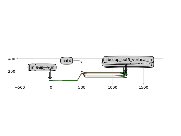
"""This example uses IoFibcoupGeneric to route all ports to fiber couplers on the same side."""
import si_fab.all as pdk  # noqa: F401
from picazzo3.filters.ring import RingRect180DropFilter

my_ring = RingRect180DropFilter()

from picazzo3.container.iofibcoup.cell import IoFibcoupGeneric

iofb = IoFibcoupGeneric(
    contents=my_ring, west_port_labels=["out1", "in1", "out2", "in2"], east_port_labels=[]
)
iofb_layout = iofb.Layout(south_east=(1200.0, 0.0), relative_offset=(0.0, 50.0), west_bundle_traces=False)

iofb_layout.visualize(annotate=True)
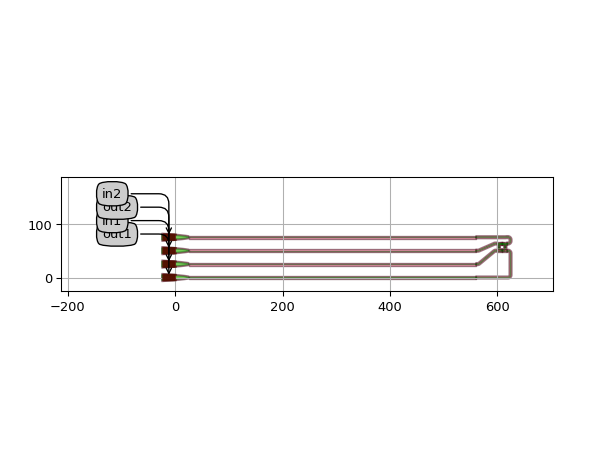
IoFibcoupEastWest
- class picazzo3.container.iofibcoup.IoFibcoupEastWest
Adapter for grating fiber couplers East and West.
The component East and West ports are treated separately, and routed towards the East and West, respectively. For this routing, they go through several steps. The settings for the East and West grating couplers can be tuned.
Here, we discuss the use for the East ports, but a similar set of parameters is available for the West ports.
First of all, the ports of the component are transitioned to a common trace template
east_trace_template. By default, it uses the standard waveguide definition defined inTECH.PCELLS.WG.DEFAULT. However, if set toNone, the trace will use the trace template of the actual port. The same holds foreast_transition_length. This can be manually specified by the user, but if a value in the list is set toNone, the default length of that type of transition will be used.Then, the ports are fanned out to the fixed
y_spacingof the fiber couplers. The length of that Fanout can be specified througheast_fanout_length. Similarly, bend radius and rounding algorithm can be set through the parameterbend_radiusandrounding_algorithm. Ifwest_bundle_tracesisTrue, the cover layers will be drawn over the Fanout. This can help reduce DRC errors.Then, the waveguides are transitioned to another waveguide template, specified in
east_connect_trace_template. By default, this is the same template aseast_trace_template, but it is possible to override it to use a lower loss multi-mode waveguide. The connection for which this waveguide is used is a simple straight connection, but depending on the chip layout it can have a long length. The transition length can be manually specified using theeast_connect_transition_length.At the output, the waveguides are transitioned to the waveguide template of the individual input and output fiber couplers. The transition length from the connection waveguide to the grating coupler can be specified using
east_fiber_coupler_transition_length.Finally, the circuit is terminated with fiber couplers, using the PCell specified in
east_fiber_coupler
The same procedure and parameters are used for the west ports
- Parameters:
- west_trace_template: ( PCell and _WaveguideTemplate ), *None allowed*
The trace template that will be used for the Fanout of the West ports. If ‘None’, the trace template of the individual port will be used. Defaults to
TECH.PCELLS.WG.DEFAULT.- east_trace_template: ( PCell and _WaveguideTemplate ), *None allowed*
The trace template that will be used for the Fanout of the East ports. If ‘None’, the trace template of the individual port will be used. Defaults to
TECH.PCELLS.WG.DEFAULT.- east_fiber_coupler_external_port_name_map: str
Dicts to map the names of the East fiber coupler ports that will be exposed as external ports. The dict is of the form {‘port_name_on_termination’: ‘unique_external_port_name’, …}. the ‘unique_external_port_name’ string can contain the identifier {port}, which will be replaced by the corresponding port name on the component. For example, the default is {‘vertical_in’ : ‘{port}’}, which will map the port ‘vertical_in’ of the fiber coupler to the name of port on the component.
- west_fiber_coupler: PCell
Fiber coupler to be attached to the West ports. Defaults to
TECH.IO.FIBCOUP.DEFAULT.PCELLS.DEFAULT_GRATING- east_fiber_coupler: PCell
Fiber coupler to be attached to the East ports. Defaults to
TECH.IO.FIBCOUP.DEFAULT.PCELLS.DEFAULT_GRATING- west_connect_trace_template: ( PCell and _WaveguideTemplate ), *None allowed*
The trace template that will be used for connecting the Fanout of the West ports. to the Grating couplers. If ‘None’, the trace template of the individual port will be used. Defaults to the same as
west_trace_template.- east_connect_trace_template: ( PCell and _WaveguideTemplate ), *None allowed*
The trace template that will be used for connecting the Fanout of the East ports. to the Grating couplers. If ‘None’, the trace template of the individual port will be used. Defaults to the same as
east_trace_template.- west_fiber_coupler_external_port_name_map: str
Dicts to map the names of the West fiber coupler ports that will be exposed as external ports. The dict is of the form {‘port_name_on_termination’: ‘unique_external_port_name’, …}. the ‘unique_external_port_name’ string can contain the identifier {port}, which will be replaced by the corresponding port name on the component. For example, the default is {‘vertical_in’ : ‘{port}’}, which will map the port ‘vertical_in’ of the fiber coupler to the name of port on the component.
- west_fiber_coupler_port_labels: List with type restriction, allowed types: <class ‘str’>
Port labels of the West fiber couplers connected to the ports of the contents. For fiber couplers with more than one port, the port labels should be concatenated with a ‘,’. For example, when using 2D grating couplers, the ports could be [‘in1,in2’, ‘in’]. This will use ports ‘in1’ and ‘in2’ of the first grating coupler, and ‘in’ of the second.By default, all the East ports of the fiber coupler are used. If an entry in the list is ‘None’, also the East ports of that fiber coupler are used. The number of entries in the list should not be identical to the number of West port. If the component has fewer West ports, only the first entries in the list will be used. If the component has more West ports, the list is just recycled. Therefore, it is allowed to use a list of just one element for multiple ports.
- east_fiber_coupler_port_labels: List with type restriction, allowed types: <class ‘str’>
Port labels of the East fiber couplers connected to the ports of the contents. For fiber couplers with more than one port, the port labels should be concatenated with a ‘,’. For example, when using 2D grating couplers, the ports could be [‘in1,in2’, ‘in’]. This will use ports ‘in1’ and ‘in2’ of the first grating coupler, and ‘in’ of the second.By default, all the West ports of all the fiber couplers are used. If an entry in the list is ‘None’, also the west ports of that fiber coupler are used. The number of entries in the list should not be identical to the number of East port. If the component has fewer East ports, only the first entries in the list will be used. If the component has more East ports, the list is just recycled. Therefore, it is allowed to use a list of just one element for multiple ports.
- west_port_labels: ( List with type restriction, allowed types: <class ‘str’> ), *None allowed*
Labels of the ports to directed to the West. Set to None to process all West ports.
- east_port_labels: ( List with type restriction, allowed types: <class ‘str’> ), *None allowed*
Labels of the ports to directed to the East. Set to None to process all East ports.
- external_port_names: str
Dictionary for remapping of the port names of the contents to the external ports
- contents: PCell
the contents of the container: the child cell
- name: String that contains only ISO/IEC 8859-1 (extended ASCII py3) or pure ASCII (py2) characters
The unique name of the pcell
- Other Parameters:
- west_trace_templates: List with type restriction, allowed types: <class ‘ipkiss3.pcell.cell.pcell.PCell’>, locked
- east_trace_templates: List with type restriction, allowed types: <class ‘ipkiss3.pcell.cell.pcell.PCell’>, locked
- west_connect_trace_templates: List with type restriction, allowed types: <class ‘ipkiss3.pcell.cell.pcell.PCell’>, locked
- east_connect_trace_templates: List with type restriction, allowed types: <class ‘ipkiss3.pcell.cell.pcell.PCell’>, locked
- west_fiber_coupler_external_port_name_maps: locked
- west_fiber_couplers: List with type restriction, allowed types: <class ‘ipkiss3.pcell.cell.pcell.PCell’>, locked
- east_fiber_coupler_external_port_name_maps: locked
- east_fiber_couplers: List with type restriction, allowed types: <class ‘ipkiss3.pcell.cell.pcell.PCell’>, locked
- port_labels: locked
Examples
"""This example illustrates how the IoFibcoupEastWest properties can customize
the routing in an IoColumn."""
import si_fab.all as pdk  # noqa: F401
from ipkiss3 import all as i3
from picazzo3.filters.mmi import MMIIdentical
from picazzo3.traces.wire_wg import WireWaveguideTemplate

wg_t1 = WireWaveguideTemplate()
wg_t1.Layout(core_width=7.0, cladding_width=8.0)
my_mmi = MMIIdentical(mmi_trace_template=wg_t1, n_inputs=1, n_outputs=5)
my_mmi.Layout(length=10.0, input_y_positions=[-1.0], output_y_positions=[-2.0, -1.0, 0.0, 1.0, 2.0])

from picazzo3.container.iofibcoup import IoFibcoupEastWest

from ipkiss3.pcell.blocks.iocolumn import IoColumn

my_column = IoColumn(name="iocol", adapter=IoFibcoupEastWest, max_n_o_lines=100)
my_column.Layout(south_east=(1200.0, 0.0))

my_column.add(my_mmi)
my_column.add(my_mmi, relative_offset=(0.0, 50.0), transformation=i3.Rotation(rotation=180.0))

layout = my_column.Layout()
layout.visualize(annotate=True)
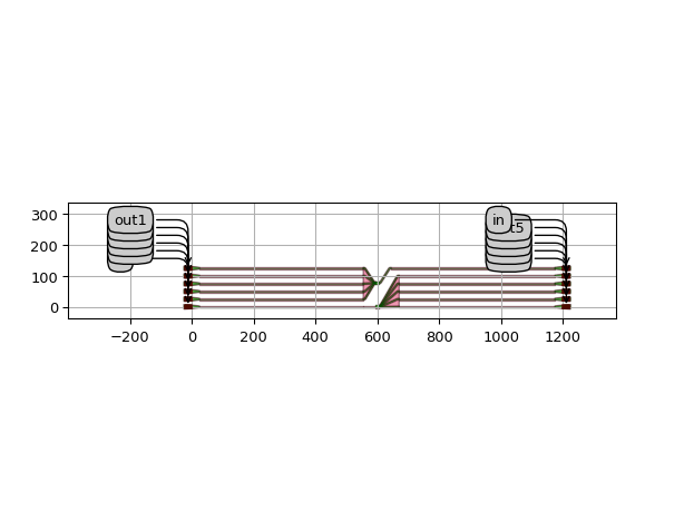
Views
- class Layout
- Parameters:
- west_connect_transition_length: ( float and Real, number and number >= 0 ), *None allowed*
The lengths of the transitions between the West fanout ports and the straight connection traces to the fiber coupler. If ‘None’, the default length for that type of transition is used.
- east_connect_transition_length: ( float and Real, number and number >= 0 ), *None allowed*
The lengths of the transitions between the East fanout ports and the straight connection traces to the fiber coupler. If ‘None’, the default length for that type of transition is used.
- west_transition_length: ( float and Real, number and number >= 0 ), *None allowed*
The lengths of the transitions between the West ports of the component and the traces of the Fanout. If ‘None’, the default length for that type of transition is used.
- east_transition_length: ( float and Real, number and number >= 0 ), *None allowed*
The lengths of the transitions between the East ports of the component and the traces of the Fanout. If ‘None’, the default length for that type of transition is used.
- west_fiber_coupler_transformation: GenericNoDistortTransform
Transformation of the West fiber coupler, relative to the y_spacing grid of the adapter. By default, no transformation is applied.
- east_fiber_coupler_transformation: GenericNoDistortTransform
Transformation of the East fiber coupler, relative to the y_spacing grid of the adapter. By default, a Horizontal Mirroring is applied.
- west_max_s_bend_angle: float and number > 0 and ]0.0,90.0]
Maximum angle for the S-bend in the fanout of the West ports.
- east_max_s_bend_angle: float and number > 0 and ]0.0,90.0]
Maximum angle for the S-bend in the fanout of the East ports.
- west_fanout_length: ( float and number > 0 ), *None allowed*
Length of the Fanout section of the West ports. If None the length will be chosen automatically.If the required length is larger than the specified length, additional space will be used.
- east_fanout_length: ( float and number > 0 ), *None allowed*
Length of the Fanout section of the East ports. If None the length will be chosen automatically.If the required length is larger than the specified length, additional space will be used.
- west_fiber_coupler_transition_length: ( float and Real, number and number >= 0 ), *None allowed*
The length of the transition between the West straight connection traces and the fiber coupler. If ‘None’, the default length for that type of transition is used.
- east_fiber_coupler_transition_length: ( float and Real, number and number >= 0 ), *None allowed*
The length of the transition between the East straight connection traces and the fiber coupler. If ‘None’, the default length for that type of transition is used.
- west_max_s_bend_angles: ]0.0,90.0]
Maximum angle for the S-bend in the fanout of the West ports.
- east_max_s_bend_angles: ]0.0,90.0]
Maximum angles for the S-bend in the fanout of the East ports.
- west_bundle_traces: ( bool, bool_ or int )
Combine the Fanout waveguides on the West in a bundle (adding Cover layers)?
- west_fanout_lengths: ( number > 0 or None )
Lengths of the waveguides in the Fanout section of the West ports. If an entry in the list is None the lengths will be chosen automatically.If the required length is larger than the specified length, additional space will be used.
- east_bundle_traces: ( bool, bool_ or int )
Combine the Fanout waveguides on the east in a bundle (adding Cover layers)?
- east_fanout_lengths: ( number > 0 or None )
Lengths of the waveguides in the Fanout section of the East ports. If an entry in the list is None the lengths will be chosen automatically.If the required length is larger than the specified length, additional space will be used.
- relative_offset: Coord2
Offset of the component as it is positioned by absolute_offset
- absolute_offset: Coord2
Offset of the component from the (0,0) of the adapter.By default this offset will be calculated such that the component ports areX-aligned around the center and that the first West port is Y-aligned to the south_west.This is after the
contents_transformationhas been applied.- contents_transformation: GenericNoDistortTransform
transformation to apply to the contents
- flatten_contents: ( bool, bool_ or int )
if True, it will insert the contents as elements in the layout, rather than as an Instance
- outline_layer: __Layer__
Layer on which to draw the block outline
- draw_block_outline: ( bool, bool_ or int )
Draw the outline of the block when set to True
- south_east: Coord2
Position of the south east corner of the block
- south_west: Coord2
Position of the south west corner of the block
- y_spacing: float and number > 0
The spacing between blocks
- view_name: String that contains only alphanumeric characters from the ASCII set or contains _$. ASCII set is extended on PY3.
The name of the view
- manhattan: ( bool, bool_ or int )
Adds rectangular blocks in the bends to avoid as much as possible non-manhattan angles.
- angle_step: float and number > 0
Angle step for rounding.
- rounding_algorithm:
Rounding algorithm used to generate the bends. Can be circular, spline, ….
- bend_radius: float and number > 0
Bend radius for the auto-generated bends.
- Other Parameters:
- west_fiber_coupler_transition_lengths: locked
- east_fiber_coupler_transition_lengths: locked
- west_connect_transition_lengths: locked
- east_connect_transition_lengths: locked
- west_transition_lengths: locked
- east_transition_lengths: locked
- west_align_fanout: locked
- east_align_fanout: locked
- west_fiber_coupler_transformations: locked
- east_fiber_coupler_transformations: locked
- south_offset: int, locked
The y-offset between south_west & south_east, measured in units of y_spacing
- width: float and Real, number and number >= 0, locked
The width of the block, calculated using south_west & south_east
Examples
"""This example illustrates the default settings of IoFibcoupEastWest ,
by adding a Ring resonator to the adapter"""
import si_fab.all as pdk  # noqa: F401
from picazzo3.filters.ring import RingRect180DropFilter

my_ring = RingRect180DropFilter()

from picazzo3.container.iofibcoup import IoFibcoupEastWest

iofb = IoFibcoupEastWest(contents=my_ring)
iofb_layout = iofb.Layout()
iofb_layout.visualize(annotate=True)

"""This example takes an MMI and encapsulates it in an IoFibcoupEastWest adapter.
It customizes several parameters of the adapter for individual tailoring of the East and West outputs."""
import si_fab.all as pdk  # noqa: F401
from ipkiss3 import all as i3
from picazzo3.filters.mmi import MMIIdentical
from picazzo3.traces.wire_wg import WireWaveguideTemplate

# normal waveguide template: single mode
wg_t = WireWaveguideTemplate()
wg_t.Layout(core_width=0.46)

# connect_template: wider to reduce losses
wgc_t = WireWaveguideTemplate()
wgc_t.Layout(core_width=2.0)

# MMI
wg_t1 = WireWaveguideTemplate()
wg_t1.Layout(core_width=7.0, cladding_width=8.0)
# input and output traces of the MMI
wg_t2 = WireWaveguideTemplate()
wg_t2.Layout(core_width=0.6)

my_mmi = MMIIdentical(
    mmi_trace_template=wg_t1,
    input_trace_template=wg_t2,
    output_trace_template=wg_t2,
    n_inputs=1,
    n_outputs=5,
)
my_mmi.Layout(length=10.0, input_y_positions=[-1.0], output_y_positions=[-2.0, -1.0, 0.0, 1.0, 2.0])

# fiber coupler
from picazzo3.fibcoup.uniform import UniformLineGrating

my_gc = UniformLineGrating(trace_template=wg_t1)

from picazzo3.container.iofibcoup import IoFibcoupEastWest

iofb = IoFibcoupEastWest(
    contents=my_mmi,  # the component
    east_trace_template=wg_t,  # trace template for East fanout
    west_trace_template=wg_t,  # trace_template for West fanout
    east_connect_trace_template=wgc_t,  # trace template for wide connections
    west_connect_trace_template=wgc_t,  # trace template for wide connections
    east_fiber_coupler=my_gc,  # fiber coupler East
    west_fiber_coupler=my_gc,
)  # fiber coupler West

iofb_layout = iofb.Layout(
    contents_transformation=i3.Rotation(rotation=-30.0),  # rotate the contents
    east_connect_transition_length=30.0,  # transition length
    # transition length between connection WG and the fiber coupler
    east_fiber_coupler_transition_length=50.0,
    south_west=(-0.0, 0.0),  # south west corner of the adapter
    south_east=(1200.0, 0.0),  # south east corner of the adapter
    relative_offset=(-100.0, 70.0),  # offset of component from the center.
)
iofb_layout.visualize(annotate=True)
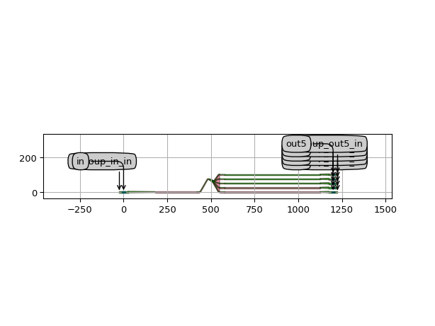
IoFibcoup
- class picazzo3.container.iofibcoup.IoFibcoup
Adapter for grating fiber couplers.
The component East and West ports are routed towards the East and West, respectively. For this routing, they go through several steps.
First of all, the ports of the component are transitioned to a common trace template
trace_template. By default, it uses the standard waveguide definition defined inTECH.PCELLS.WG.DEFAULT. However, if set toNone, the trace will use the trace template of the actual port. The same holds fortransition_length. This can be manually specified by the user, but if a value in the list is set toNone, the default length of that type of transition will be used.Then, the ports are fanned out to the fixed
y_spacingof the fiber couplers. The length of that Fanout can be specified throughfanout_length. Similarly, bend radius and rounding algorithm can be set through the parameterbend_radiusandrounding_algorithm. Ifbundle_tracesisTrue, the cover layers will be drawn over the Fanout. This can help reduce DRC errors.Then, the waveguides are transitioned to another waveguide template, specified in
east_connect_trace_template. By default, this is the same template astrace_template, but it is possible to override it to use a lower loss multi-mode waveguide. The connection for which this waveguide is used is a simple straight connection, but depending on the chip layout it can have a long length. The transition length can be manually specified using theconnect_transition_length.At the output, the waveguides are transitioned to the waveguide template of the individual input and output fiber couplers. The transition length from the connection waveguide to the grating coupler can be specified using
fiber_coupler_transition_length.Finally, the circuit is terminated with fiber couplers, using the PCell specified in
fiber_coupler
- Parameters:
- trace_template: ( PCell and _WaveguideTemplate ), *None allowed*
The trace template that will be used for the Fanout of the East and West ports. If ‘None’, the trace template of the individual port will be used. Defaults to
TECH.PCELLS.WG.DEFAULT.- fiber_coupler_external_port_name_map: str
Dicts to map the names of the fiber coupler ports that will be exposed as external ports. The dict is of the form {‘port_name_on_termination’: ‘unique_external_port_name’, …}. the ‘unique_external_port_name’ string can contain the identifier {port}, which will be replaced by the corresponding port name on the component. For example, the default is {‘vertical_in’ : ‘{port}’}, which will map the port ‘vertical_in’ of the fiber coupler to the name of port on the component.
- connect_trace_template: ( PCell and _WaveguideTemplate ), *None allowed*
The trace template that will be used for connecting the Fanout of the East and West ports. to the Grating couplers. If ‘None’, the trace template of the individual port will be used. Defaults to the same as
trace_template.- fiber_coupler: PCell
Fiber coupler to be attached to the East and West ports. Defaults to
TECH.IO.FIBCOUP.DEFAULT.PCELLS.DEFAULT_GRATING- west_fiber_coupler_port_labels: List with type restriction, allowed types: <class ‘str’>
Port labels of the West fiber couplers connected to the ports of the contents. For fiber couplers with more than one port, the port labels should be concatenated with a ‘,’. For example, when using 2D grating couplers, the ports could be [‘in1,in2’, ‘in’]. This will use ports ‘in1’ and ‘in2’ of the first grating coupler, and ‘in’ of the second.By default, all the East ports of the fiber coupler are used. If an entry in the list is ‘None’, also the East ports of that fiber coupler are used. The number of entries in the list should not be identical to the number of West port. If the component has fewer West ports, only the first entries in the list will be used. If the component has more West ports, the list is just recycled. Therefore, it is allowed to use a list of just one element for multiple ports.
- east_fiber_coupler_port_labels: List with type restriction, allowed types: <class ‘str’>
Port labels of the East fiber couplers connected to the ports of the contents. For fiber couplers with more than one port, the port labels should be concatenated with a ‘,’. For example, when using 2D grating couplers, the ports could be [‘in1,in2’, ‘in’]. This will use ports ‘in1’ and ‘in2’ of the first grating coupler, and ‘in’ of the second.By default, all the West ports of all the fiber couplers are used. If an entry in the list is ‘None’, also the west ports of that fiber coupler are used. The number of entries in the list should not be identical to the number of East port. If the component has fewer East ports, only the first entries in the list will be used. If the component has more East ports, the list is just recycled. Therefore, it is allowed to use a list of just one element for multiple ports.
- west_port_labels: ( List with type restriction, allowed types: <class ‘str’> ), *None allowed*
Labels of the ports to directed to the West. Set to None to process all West ports.
- east_port_labels: ( List with type restriction, allowed types: <class ‘str’> ), *None allowed*
Labels of the ports to directed to the East. Set to None to process all East ports.
- external_port_names: str
Dictionary for remapping of the port names of the contents to the external ports
- contents: PCell
the contents of the container: the child cell
- name: String that contains only ISO/IEC 8859-1 (extended ASCII py3) or pure ASCII (py2) characters
The unique name of the pcell
- Other Parameters:
- west_trace_template: PCell and _WaveguideTemplate, locked
- east_trace_template: PCell and _WaveguideTemplate, locked
- west_trace_templates: List with type restriction, allowed types: <class ‘ipkiss3.pcell.cell.pcell.PCell’>, locked
- east_trace_templates: List with type restriction, allowed types: <class ‘ipkiss3.pcell.cell.pcell.PCell’>, locked
- west_fiber_coupler: PCell, locked
- east_fiber_coupler: PCell, locked
- west_fiber_coupler_external_port_name_map: locked
- west_connect_trace_template: PCell and _WaveguideTemplate, locked
- east_connect_trace_template: PCell and _WaveguideTemplate, locked
- east_fiber_coupler_external_port_name_map: locked
- west_connect_trace_templates: List with type restriction, allowed types: <class ‘ipkiss3.pcell.cell.pcell.PCell’>, locked
- east_connect_trace_templates: List with type restriction, allowed types: <class ‘ipkiss3.pcell.cell.pcell.PCell’>, locked
- west_fiber_coupler_external_port_name_maps: locked
- west_fiber_couplers: List with type restriction, allowed types: <class ‘ipkiss3.pcell.cell.pcell.PCell’>, locked
- east_fiber_coupler_external_port_name_maps: locked
- east_fiber_couplers: List with type restriction, allowed types: <class ‘ipkiss3.pcell.cell.pcell.PCell’>, locked
- port_labels: locked
Examples
"""This example illustrates how the IoFibcoup properties can customize
the routing in an IoColumn."""
import si_fab.all as pdk  # noqa: F401
from ipkiss3 import all as i3
from picazzo3.filters.mmi import MMIIdentical
from picazzo3.traces.wire_wg import WireWaveguideTemplate

wg_t1 = WireWaveguideTemplate()
wg_t1.Layout(core_width=7.0, cladding_width=8.0)
my_mmi = MMIIdentical(mmi_trace_template=wg_t1, n_inputs=1, n_outputs=5)
my_mmi.Layout(length=10.0, input_y_positions=[-1.0], output_y_positions=[-2.0, -1.0, 0.0, 1.0, 2.0])

from picazzo3.container.iofibcoup import IoFibcoup

from ipkiss3.pcell.blocks.iocolumn import IoColumn

my_column = IoColumn(name="iocol", adapter=IoFibcoup, max_n_o_lines=100)
layout = my_column.Layout(south_east=(1400.0, 0.0))

my_column.add(my_mmi)
my_column.add(my_mmi, relative_offset=(0.0, 50.0), transformation=i3.Rotation(rotation=180.0))

layout.visualize(annotate=True)
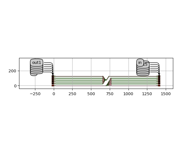
Views
- class Layout
- Parameters:
- fiber_coupler_transition_length: ( float and Real, number and number >= 0 ), *None allowed*
The length of the transition between the straight connection traces and the fiber coupler. If ‘None’, the default length for that type of transition is used.
- connect_transition_length: ( float and Real, number and number >= 0 ), *None allowed*
The length of the transitions between the fanout ports and the straight connection traces to the fiber coupler. If ‘None’, the default length for that type of transition is used.
- transition_length: ( float and Real, number and number >= 0 ), *None allowed*
The lengths of the transitions between the East and West ports of the component and the traces of the Fanout. If ‘None’, the default length for that type of transition is used.
- max_s_bend_angle: float and number > 0 and ]0.0,90.0]
Maximum angle for the S-bend in the fanout.
- fanout_length: float and number > 0
Length of the Fanout section
- bundle_traces: ( bool, bool_ or int )
Combine the Fanout waveguides on the east in a bundle (adding Cover layers)?
- west_max_s_bend_angle: float and number > 0 and ]0.0,90.0]
Maximum angle for the S-bend in the fanout of the West ports.
- east_max_s_bend_angle: float and number > 0 and ]0.0,90.0]
Maximum angle for the S-bend in the fanout of the East ports.
- fiber_coupler_transformation: GenericNoDistortTransform
Transformation of the fiber coupler, relative to the y_spacing grid of the adapter. By default, an additional Horizontal Mirroring is applied to the East fiber coupler
- west_max_s_bend_angles: ]0.0,90.0]
Maximum angle for the S-bend in the fanout of the West ports.
- east_max_s_bend_angles: ]0.0,90.0]
Maximum angles for the S-bend in the fanout of the East ports.
- west_fanout_lengths: ( number > 0 or None )
Lengths of the waveguides in the Fanout section of the West ports. If an entry in the list is None the lengths will be chosen automatically.If the required length is larger than the specified length, additional space will be used.
- east_fanout_lengths: ( number > 0 or None )
Lengths of the waveguides in the Fanout section of the East ports. If an entry in the list is None the lengths will be chosen automatically.If the required length is larger than the specified length, additional space will be used.
- relative_offset: Coord2
Offset of the component as it is positioned by absolute_offset
- absolute_offset: Coord2
Offset of the component from the (0,0) of the adapter.By default this offset will be calculated such that the component ports areX-aligned around the center and that the first West port is Y-aligned to the south_west.This is after the
contents_transformationhas been applied.- contents_transformation: GenericNoDistortTransform
transformation to apply to the contents
- flatten_contents: ( bool, bool_ or int )
if True, it will insert the contents as elements in the layout, rather than as an Instance
- outline_layer: __Layer__
Layer on which to draw the block outline
- draw_block_outline: ( bool, bool_ or int )
Draw the outline of the block when set to True
- south_east: Coord2
Position of the south east corner of the block
- south_west: Coord2
Position of the south west corner of the block
- y_spacing: float and number > 0
The spacing between blocks
- view_name: String that contains only alphanumeric characters from the ASCII set or contains _$. ASCII set is extended on PY3.
The name of the view
- manhattan: ( bool, bool_ or int )
Adds rectangular blocks in the bends to avoid as much as possible non-manhattan angles.
- angle_step: float and number > 0
Angle step for rounding.
- rounding_algorithm:
Rounding algorithm used to generate the bends. Can be circular, spline, ….
- bend_radius: float and number > 0
Bend radius for the auto-generated bends.
- Other Parameters:
- east_fiber_coupler_transition_length: locked
- west_connect_transition_length: locked
- east_connect_transition_length: locked
- west_fiber_coupler_transition_lengths: locked
- east_fiber_coupler_transition_lengths: locked
- west_connect_transition_lengths: locked
- east_connect_transition_lengths: locked
- west_transition_length: locked
- east_transition_length: locked
- west_transition_lengths: locked
- east_transition_lengths: locked
- west_fanout_length: locked
- east_fanout_length: locked
- west_fiber_coupler_transition_length: locked
- west_fiber_coupler_transformation: locked
- east_fiber_coupler_transformation: locked
- west_bundle_traces: locked
- west_align_fanout: locked
- east_align_fanout: locked
- east_bundle_traces: locked
- west_fiber_coupler_transformations: locked
- east_fiber_coupler_transformations: locked
- south_offset: int, locked
The y-offset between south_west & south_east, measured in units of y_spacing
- width: float and Real, number and number >= 0, locked
The width of the block, calculated using south_west & south_east
Examples
"""This example illustrates the default settings of IoFibcoup,
by adding a Ring resonator to the adapter"""
import si_fab.all as pdk  # noqa: F401
from picazzo3.filters.ring import RingRect180DropFilter

my_ring = RingRect180DropFilter()

from picazzo3.container.iofibcoup import IoFibcoup

iofb = IoFibcoup(contents=my_ring)
iofb_layout = iofb.Layout()

iofb_layout.visualize(annotate=True)

"""This example takes an MMI and encapsulates it in an IoFibcoupadapter.
It customizes several parameters of the adapter for individual tailoring of the East and West outputs."""
import si_fab.all as pdk  # noqa: F401
from ipkiss3 import all as i3
from picazzo3.filters.mmi import MMIIdentical
from picazzo3.traces.wire_wg import WireWaveguideTemplate

# normal waveguide template: single mode
wg_t = WireWaveguideTemplate()
wg_t.Layout(core_width=0.46)

# connect_template: wider to reduce losses
wgc_t = WireWaveguideTemplate()
wgc_t.Layout(core_width=2.0)

# MMI
wg_t1 = WireWaveguideTemplate()
wg_t1.Layout(core_width=7.0, cladding_width=8.0)
# input and output traces of the MMI
wg_t2 = WireWaveguideTemplate()
wg_t2.Layout(core_width=0.6)

my_mmi = MMIIdentical(
    mmi_trace_template=wg_t1,
    input_trace_template=wg_t2,
    output_trace_template=wg_t2,
    n_inputs=1,
    n_outputs=5,
)
my_mmi.Layout(length=10.0, input_y_positions=[-1.0], output_y_positions=[-2.0, -1.0, 0.0, 1.0, 2.0])

# fiber coupler
from picazzo3.fibcoup.uniform import UniformLineGrating

my_gc = UniformLineGrating(trace_template=wg_t1)

from picazzo3.container.iofibcoup import IoFibcoup

iofb = IoFibcoup(
    contents=my_mmi,  # the component
    trace_template=wg_t,  # trace template for fanout
    connect_trace_template=wgc_t,  # trace template for wide connections
    fiber_coupler=my_gc,  # fiber coupler
)

iofb_layout = iofb.Layout(
    contents_transformation=i3.Rotation(rotation=-10.0),  # rotate the contents
    connect_transition_length=30.0,  # transition length
    fiber_coupler_transition_length=50.0,  # transition length between connection WG and the fiber coupler
    south_west=(-0.0, 0.0),  # south west corner of the adapter
    south_east=(1200.0, 0.0),  # south east corner of the adapter
    relative_offset=(0.0, 70.0),  # offset of component from the center.
)
iofb_layout.visualize(annotate=True)
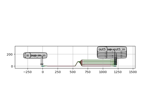
"""This example shows how to use fiber couplers that don't have their waveguide port facing towards the east.

We use a fiber coupler with both an east-facing and a west-facing port here,
but this example can easily be applied to other couplers.
"""

import si_fab.all as pdk  # noqa: F401
from ipkiss3 import all as i3
from picazzo3.filters.mmi import MMI1x2
from picazzo3.traces.wire_wg import WireWaveguideTemplate

# normal waveguide template: single mode
wg_t = WireWaveguideTemplate()
wg_t.Layout(core_width=0.46)

# MMI
wg_t1 = WireWaveguideTemplate()
wg_t1.Layout(core_width=7.0, cladding_width=8.0)
# input and output traces of the MMI
wg_t2 = WireWaveguideTemplate()
wg_t2.Layout(core_width=0.6)

my_mmi = MMI1x2(
    mmi_trace_template=wg_t1,
    input_trace_template=wg_t2,
    output_trace_template=wg_t2,
)
my_mmi.Layout(length=10.0, trace_spacing=2.0)

# fiber coupler
from picazzo3.fibcoup.uniform import UniformLineGrating

my_gc = UniformLineGrating(trace_template=wg_t1)

from picazzo3.container.iofibcoup import IoFibcoup

# we want to use the west-facing 'in' port of the fiber coupler

iofb = IoFibcoup(
    contents=my_mmi,  # the component
    trace_template=wg_t,  # trace template for fanout
    fiber_coupler=my_gc,  # fiber coupler
    west_fiber_coupler_port_labels=["in"],
    east_fiber_coupler_port_labels=["in"],
)

iofb_layout = iofb.Layout(
    south_west=(0.0, 0.0),  # south west corner of the adapter
    south_east=(500.0, 0.0),  # south east corner of the adapter
    # we need to mirror the fiber coupler so the 'in' port faces east
    fiber_coupler_transformation=i3.HMirror(),
)
iofb_layout.visualize(annotate=True)
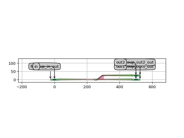
ContainerWithWaveguides
ContainerWithWaveguides
- class picazzo3.container.container_waveguides.ContainerWithWaveguides
Abstract base class for containers which add waveguides to the contents, such as fanout or for routing ports in certain directions
Waveguides are provided as a list of child cells. They will be bundled if bundled=True.
- Parameters:
- trace_template: ( PCell and _WaveguideTemplate ), *None allowed*
Template for all ports, defaults to TECH.PCELLS.WG.DEFAULT.When set to None, the waveguide templates of the ports will be used.
- waveguides: List with type restriction, allowed types: <class ‘ipkiss3.pcell.cell.pcell.PCell’>
waveguides added to the contents
- auto_transition: ( bool, bool_ or int )
If True, automatically transition all ports of contents to the given trace template. If False, no transitions are applied, which might lead to a discontinuity in the waveguide. Also, if trace_template is None, no transitions are applied.
- port_labels: ( List with type restriction, allowed types: <class ‘str’> ), *None allowed*
Labels of the ports to be processed. Set to None to process all ports.
- external_port_names: str
Dictionary for remapping of the port names of the contents to the external ports
- contents: PCell
the contents of the container: the child cell
- name: String that contains only ISO/IEC 8859-1 (extended ASCII py3) or pure ASCII (py2) characters
The unique name of the pcell
- Other Parameters:
- trace_templates: List with type restriction, allowed types: <class ‘ipkiss3.pcell.cell.pcell.PCell’>, locked
list of templates to apply to all ports
Examples
import si_fab.all as pdk  # noqa: F401
from picazzo3.filters.ring import RingRect180DropFilter
from picazzo3.container.container_waveguides import ContainerWithWaveguides
from ipkiss3 import all as i3

my_ring = RingRect180DropFilter(name="my_ring1")
my_ring_layout = my_ring.Layout()

port_labels = ["E1", "W0"]

wgs = []
for pl in port_labels:
    p = my_ring_layout.ports[pl]
    shape = i3.Shape(points=[p.position])
    shape.add_polar(10.0, p.angle_deg)
    wg = i3.Waveguide()
    wg.Layout(shape=shape)
    wgs.append(wg)

my_container = ContainerWithWaveguides(
    name="my_waveguide_container1", contents=my_ring, waveguides=wgs, port_labels=port_labels
)
layout = my_container.Layout()
layout.visualize(annotate=True)
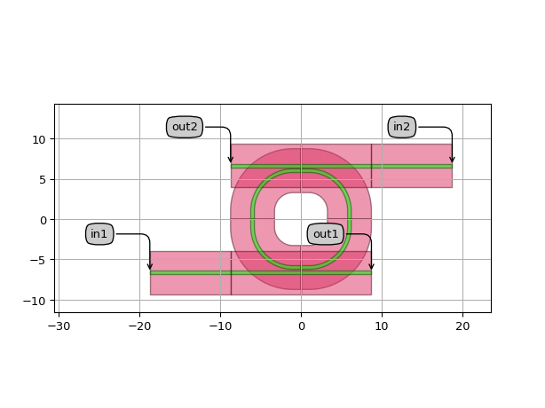
Views
- class Layout
- Parameters:
- routes:
routes along which the waveguides will be generated
- contents_transformation: GenericNoDistortTransform
transformation to apply to the contents
- flatten_contents: ( bool, bool_ or int )
if True, it will insert the contents as elements in the layout, rather than as an Instance
- view_name: String that contains only alphanumeric characters from the ASCII set or contains _$. ASCII set is extended on PY3.
The name of the view
ContainerWithWaveguideBundle
- class picazzo3.container.container_waveguides.ContainerWithWaveguideBundle
Abstract base class for containers which add waveguides to the contents, such as fanout or for routing ports in certain directions
Waveguides are provided as a list of child cells. They will be bundled if bundled = True.
- Parameters:
- trace_template: ( PCell and _WaveguideTemplate ), *None allowed*
Template for all ports, defaults to TECH.PCELLS.WG.DEFAULT.When set to None, the waveguide templates of the ports will be used.
- waveguides: List with type restriction, allowed types: <class ‘ipkiss3.pcell.cell.pcell.PCell’>
waveguides added to the contents
- auto_transition: ( bool, bool_ or int )
If True, automatically transition all ports of contents to the given trace template. If False, no transitions are applied, which might lead to a discontinuity in the waveguide. Also, if trace_template is None, no transitions are applied.
- port_labels: ( List with type restriction, allowed types: <class ‘str’> ), *None allowed*
Labels of the ports to be processed. Set to None to process all ports.
- external_port_names: str
Dictionary for remapping of the port names of the contents to the external ports
- contents: PCell
the contents of the container: the child cell
- name: String that contains only ISO/IEC 8859-1 (extended ASCII py3) or pure ASCII (py2) characters
The unique name of the pcell
- Other Parameters:
- bundle: ( PCell ), locked, *None allowed*
bundle of waveguides added to the contents, generated based on the supplied waveguides list
- trace_templates: List with type restriction, allowed types: <class ‘ipkiss3.pcell.cell.pcell.PCell’>, locked
list of templates to apply to all ports
Views
- class Layout
- Parameters:
- area_layer_on: ( bool, bool_ or int )
When True, the waveguide area will be covered by i3.Rectangles on all cover layers.
- routes:
routes along which the waveguides will be generated
- contents_transformation: GenericNoDistortTransform
transformation to apply to the contents
- flatten_contents: ( bool, bool_ or int )
if True, it will insert the contents as elements in the layout, rather than as an Instance
- view_name: String that contains only alphanumeric characters from the ASCII set or contains _$. ASCII set is extended on PY3.
The name of the view
ContainerWithRoundedWaveguides
- class picazzo3.container.container_waveguides.ContainerWithRoundedWaveguides
Container with waveguides (
picazzo3.container.container_waveguides.ContainerWithWaveguides) which generates its waveguides from a given waveguide_template and routes. You can specify a bend radius and rounding algorithm for the waveguides in the Layout view.- Parameters:
- trace_template: ( PCell and _WaveguideTemplate ), *None allowed*
Template for all ports, defaults to TECH.PCELLS.WG.DEFAULT.When set to None, the waveguide templates of the ports will be used.
- auto_transition: ( bool, bool_ or int )
If True, automatically transition all ports of contents to the given trace template. If False, no transitions are applied, which might lead to a discontinuity in the waveguide. Also, if trace_template is None, no transitions are applied.
- port_labels: ( List with type restriction, allowed types: <class ‘str’> ), *None allowed*
Labels of the ports to be processed. Set to None to process all ports.
- external_port_names: str
Dictionary for remapping of the port names of the contents to the external ports
- contents: PCell
the contents of the container: the child cell
- name: String that contains only ISO/IEC 8859-1 (extended ASCII py3) or pure ASCII (py2) characters
The unique name of the pcell
- Other Parameters:
- waveguides: List with type restriction, allowed types: <class ‘ipkiss3.pcell.cell.pcell.PCell’>, locked
- trace_templates: List with type restriction, allowed types: <class ‘ipkiss3.pcell.cell.pcell.PCell’>, locked
list of templates to apply to all ports
Examples
import si_fab.all as pdk  # noqa: F401
from picazzo3.filters.ring import RingRect180DropFilter
from picazzo3.container.container_waveguides import ContainerWithRoundedWaveguides
from ipkiss3 import all as i3

my_ring = RingRect180DropFilter(name="my_ring3")
my_ring_layout = my_ring.Layout()

port_labels = ["E1", "W0"]

shapes = []
for pl in port_labels:
    p = my_ring_layout.ports[pl]
    shape = i3.Shape(points=[p.position])
    shape.add_polar(15.0, p.angle_deg)
    shape.add_polar(15.0, p.angle_deg + 90.0)
    shapes.append(shape)

my_container = ContainerWithRoundedWaveguides(
    name="my_waveguide_container3", contents=my_ring, port_labels=port_labels
)
layout = my_container.Layout(routes=shapes, bend_radius=10.0)

layout.visualize(annotate=True)
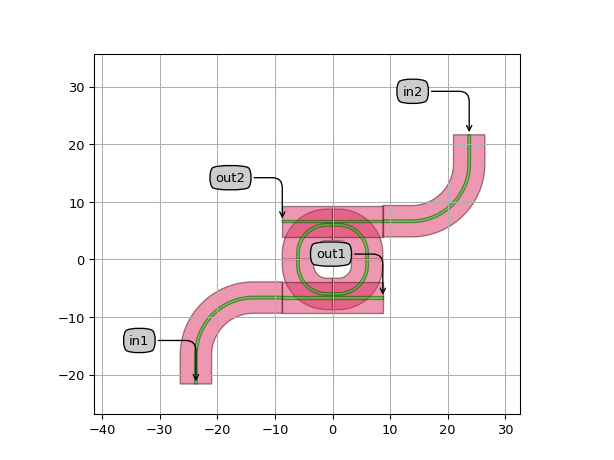
Views
- class Layout
- Parameters:
- routes:
routes along which the waveguides will be generated
- contents_transformation: GenericNoDistortTransform
transformation to apply to the contents
- flatten_contents: ( bool, bool_ or int )
if True, it will insert the contents as elements in the layout, rather than as an Instance
- view_name: String that contains only alphanumeric characters from the ASCII set or contains _$. ASCII set is extended on PY3.
The name of the view
- manhattan: ( bool, bool_ or int )
Adds rectangular blocks in the bends to avoid as much as possible non-manhattan angles.
- angle_step: float and number > 0
Angle step for rounding.
- rounding_algorithm:
Rounding algorithm used to generate the bends. Can be circular, spline, ….
- bend_radius: float and number > 0
Bend radius for the auto-generated bends.
ContainerWithRoundedWaveguideBundle
- class picazzo3.container.container_waveguides.ContainerWithRoundedWaveguideBundle
Container with waveguide bundle (
picazzo3.container.container_waveguides.ContainerWithWaveguideBundle) which generates its waveguides from a given waveguide_template and routes and rounds the bends. You can specify a bend radius and rounding algorithm for the waveguides in the Layout view.- Parameters:
- trace_template: ( PCell and _WaveguideTemplate ), *None allowed*
Template for all ports, defaults to TECH.PCELLS.WG.DEFAULT.When set to None, the waveguide templates of the ports will be used.
- auto_transition: ( bool, bool_ or int )
If True, automatically transition all ports of contents to the given trace template. If False, no transitions are applied, which might lead to a discontinuity in the waveguide. Also, if trace_template is None, no transitions are applied.
- port_labels: ( List with type restriction, allowed types: <class ‘str’> ), *None allowed*
Labels of the ports to be processed. Set to None to process all ports.
- external_port_names: str
Dictionary for remapping of the port names of the contents to the external ports
- contents: PCell
the contents of the container: the child cell
- name: String that contains only ISO/IEC 8859-1 (extended ASCII py3) or pure ASCII (py2) characters
The unique name of the pcell
- Other Parameters:
- bundle: ( PCell ), locked, *None allowed*
bundle of waveguides added to the contents, generated based on the supplied waveguides list
- waveguides: List with type restriction, allowed types: <class ‘ipkiss3.pcell.cell.pcell.PCell’>, locked
- trace_templates: List with type restriction, allowed types: <class ‘ipkiss3.pcell.cell.pcell.PCell’>, locked
list of templates to apply to all ports
Examples
import si_fab.all as pdk  # noqa: F401
from picazzo3.filters.ring import RingRect180DropFilter
from picazzo3.container.container_waveguides import ContainerWithRoundedWaveguideBundle
from ipkiss3 import all as i3

my_ring = RingRect180DropFilter(name="my_ring_4")
my_ring_layout = my_ring.Layout()

port_labels = ["E0", "E1"]

shapes = []
for pl in port_labels:
    p = my_ring_layout.ports[pl]
    shape = i3.Shape(points=[p.position])
    shape.add_polar(15.0, p.angle_deg)
    shape.add_polar(15.0, p.angle_deg + 30.0)
    shapes.append(shape)

my_container = ContainerWithRoundedWaveguideBundle(
    name="my_waveguide_container_4", contents=my_ring, port_labels=port_labels
)
layout = my_container.Layout(routes=shapes, bend_radius=10.0, area_layer_on=True)
layout.visualize(annotate=True)
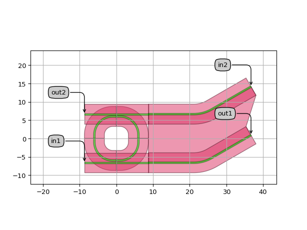
Views
- class Layout
- Parameters:
- area_layer_on: ( bool, bool_ or int )
When True, the waveguide area will be covered by i3.Rectangles on all cover layers.
- routes:
routes along which the waveguides will be generated
- contents_transformation: GenericNoDistortTransform
transformation to apply to the contents
- flatten_contents: ( bool, bool_ or int )
if True, it will insert the contents as elements in the layout, rather than as an Instance
- view_name: String that contains only alphanumeric characters from the ASCII set or contains _$. ASCII set is extended on PY3.
The name of the view
- manhattan: ( bool, bool_ or int )
Adds rectangular blocks in the bends to avoid as much as possible non-manhattan angles.
- angle_step: float and number > 0
Angle step for rounding.
- rounding_algorithm:
Rounding algorithm used to generate the bends. Can be circular, spline, ….
- bend_radius: float and number > 0
Bend radius for the auto-generated bends.
ExtendPorts
ExtendPorts
- class picazzo3.container.extend_ports.ExtendPorts
Extends all the ports listed in
port_labelswith a waveguide of a given length.This length is specified in
extension_lengthof the Layout View.A common trace template for all ports is specified through
trace_template. When this is set to None (the default), the trace templates of the ports of the contents will be used.- Parameters:
- trace_template: ( PCell and _WaveguideTemplate ), *None allowed*
Template for all ports. If None, the trace templates of the ports will be used
- waveguides: List with type restriction, allowed types: <class ‘ipkiss3.pcell.cell.pcell.PCell’>
waveguides added to the contents
- auto_transition: ( bool, bool_ or int )
If True, automatically transition all ports of contents to the given trace template. If False, no transitions are applied, which might lead to a discontinuity in the waveguide. Also, if trace_template is None, no transitions are applied.
- port_labels: ( List with type restriction, allowed types: <class ‘str’> ), *None allowed*
Labels of the ports to be processed. Set to None to process all ports.
- external_port_names: str
Dictionary for remapping of the port names of the contents to the external ports
- contents: PCell
the contents of the container: the child cell
- name: String that contains only ISO/IEC 8859-1 (extended ASCII py3) or pure ASCII (py2) characters
The unique name of the pcell
- Other Parameters:
- bundle: ( PCell ), locked, *None allowed*
bundle of waveguides added to the contents, generated based on the supplied waveguides list
- trace_templates: List with type restriction, allowed types: <class ‘ipkiss3.pcell.cell.pcell.PCell’>, locked
list of templates to apply to all ports
Views
- class Layout
- Parameters:
- extension_length: float and number > 0
Length by which the ports are extended
- area_layer_on: ( bool, bool_ or int )
When True, the waveguide area will be covered by i3.Rectangles on all cover layers.
- routes:
routes along which the waveguides will be generated
- contents_transformation: GenericNoDistortTransform
transformation to apply to the contents
- flatten_contents: ( bool, bool_ or int )
if True, it will insert the contents as elements in the layout, rather than as an Instance
- view_name: String that contains only alphanumeric characters from the ASCII set or contains _$. ASCII set is extended on PY3.
The name of the view
- Other Parameters:
- extension_lengths: locked
Examples
import si_fab.all as pdk  # noqa: F401
from picazzo3.filters.ring import RingRect180DropFilter
from picazzo3.traces.wire_wg import WireWaveguideTemplate
from picazzo3.container.extend_ports import ExtendPorts

wg_t1 = WireWaveguideTemplate()
wg_t1.Layout(core_width=0.55)
wg_t2 = WireWaveguideTemplate()
wg_t2.Layout(core_width=0.35)

my_ring = RingRect180DropFilter(name="ring_for_fanout", coupler_trace_templates=[wg_t1, wg_t2])
my_ring.Layout()

port_labels = ["E1", "E0"]

my_container = ExtendPorts(contents=my_ring, port_labels=port_labels, auto_transition=True)
layout = my_container.Layout(extension_length=20.0, area_layer_on=False)
layout.visualize(annotate=True)
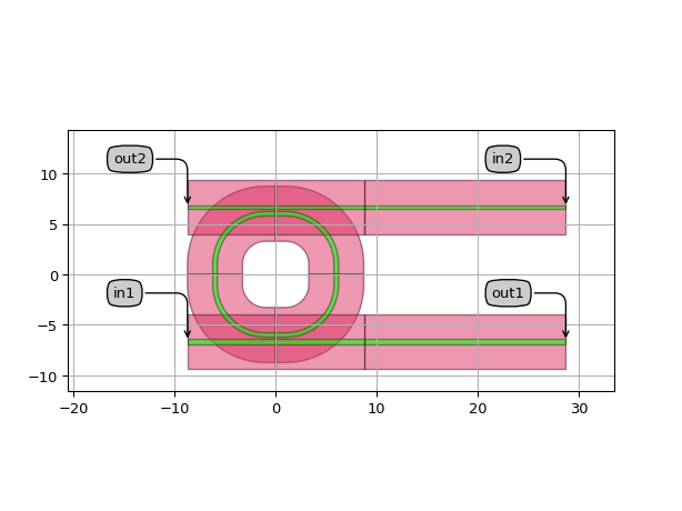
import si_fab.all as pdk  # noqa: F401
from picazzo3.filters.ring import RingRect180DropFilter
from picazzo3.traces.wire_wg import WireWaveguideTemplate
from picazzo3.container.extend_ports import ExtendPorts

wg_t1 = WireWaveguideTemplate()
wg_t1.Layout(core_width=0.55)
wg_t2 = WireWaveguideTemplate()
wg_t2.Layout(core_width=0.35)

my_ring = RingRect180DropFilter(name="ring_for_fanout", coupler_trace_templates=[wg_t1, wg_t2])
my_ring.Layout()

port_labels = ["E1", "E0"]

my_container = ExtendPorts(
    contents=my_ring, port_labels=port_labels, trace_template=wg_t1, auto_transition=False  # Default
)
layout = my_container.Layout(extension_length=20.0, area_layer_on=True)
layout.visualize(annotate=True)
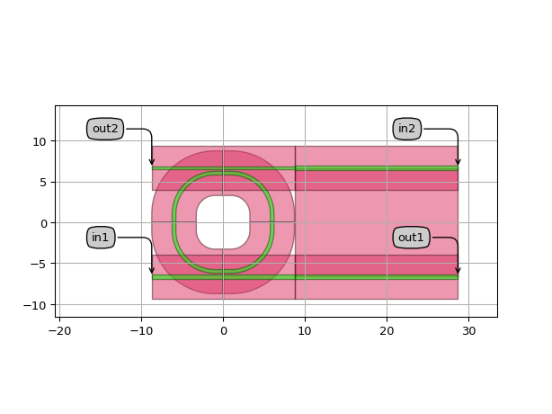
Route Ports
RoutePortsEastWest
- class picazzo3.container.route_ports.RoutePortsEastWest
Routes ports to the east or west side of a component
- Parameters:
- west_port_labels: ( List with type restriction, allowed types: <class ‘str’> ), *None allowed*
Labels of the ports to directed to the West. Set to None to process all West ports.
- east_port_labels: ( List with type restriction, allowed types: <class ‘str’> ), *None allowed*
Labels of the ports to directed to the East. Set to None to process all East ports.
- trace_template: ( PCell and _WaveguideTemplate ), *None allowed*
Template for all ports, defaults to TECH.PCELLS.WG.DEFAULT.When set to None, the waveguide templates of the ports will be used.
- auto_transition: ( bool, bool_ or int )
If True, automatically transition all ports of contents to the given trace template. If False, no transitions are applied, which might lead to a discontinuity in the waveguide. Also, if trace_template is None, no transitions are applied.
- external_port_names: str
Dictionary for remapping of the port names of the contents to the external ports
- contents: PCell
the contents of the container: the child cell
- name: String that contains only ISO/IEC 8859-1 (extended ASCII py3) or pure ASCII (py2) characters
The unique name of the pcell
- Other Parameters:
- bundle: ( PCell ), locked, *None allowed*
bundle of waveguides added to the contents, generated based on the supplied waveguides list
- waveguides: List with type restriction, allowed types: <class ‘ipkiss3.pcell.cell.pcell.PCell’>, locked
- trace_templates: List with type restriction, allowed types: <class ‘ipkiss3.pcell.cell.pcell.PCell’>, locked
list of templates to apply to all ports
- port_labels: locked
Views
- class Layout
- Parameters:
- target_coordinate_west: ( float ), *None allowed*
The coordinate where the west routes are aligned
- target_coordinate_east: ( float ), *None allowed*
The coordinate where the east routes are aligned
- reference_west: str and String that contains only ISO/IEC 8859-1 (extended ASCII py3) or pure ASCII (py2) characters
Port Label of port that serves as y reference
- reference_east: str and String that contains only ISO/IEC 8859-1 (extended ASCII py3) or pure ASCII (py2) characters
Port Label of port that serves as y reference
- spacing: float and number > 0
Distance between the endpoints of the routes
- area_layer_on: ( bool, bool_ or int )
When True, the waveguide area will be covered by i3.Rectangles on all cover layers.
- contents_transformation: GenericNoDistortTransform
transformation to apply to the contents
- flatten_contents: ( bool, bool_ or int )
if True, it will insert the contents as elements in the layout, rather than as an Instance
- view_name: String that contains only alphanumeric characters from the ASCII set or contains _$. ASCII set is extended on PY3.
The name of the view
- manhattan: ( bool, bool_ or int )
Adds rectangular blocks in the bends to avoid as much as possible non-manhattan angles.
- angle_step: float and number > 0
Angle step for rounding.
- rounding_algorithm:
Rounding algorithm used to generate the bends. Can be circular, spline, ….
- bend_radius: float and number > 0
Bend radius for the auto-generated bends.
- Other Parameters:
- routes: locked
Examples
import si_fab.all as pdk  # noqa: F401
from picazzo3.filters.ring import RingRect180DropFilter
from picazzo3.container.route_ports import RoutePortsEastWest

my_ring = RingRect180DropFilter()

my_ring_ew = RoutePortsEastWest(
    contents=my_ring,
    east_port_labels=["E0", "E1", "W1"],  # ports to be routed eastwards
    west_port_labels=["W0"],  # ports to be routed westward
)
layout = my_ring_ew.Layout()
layout.visualize(annotate=True)
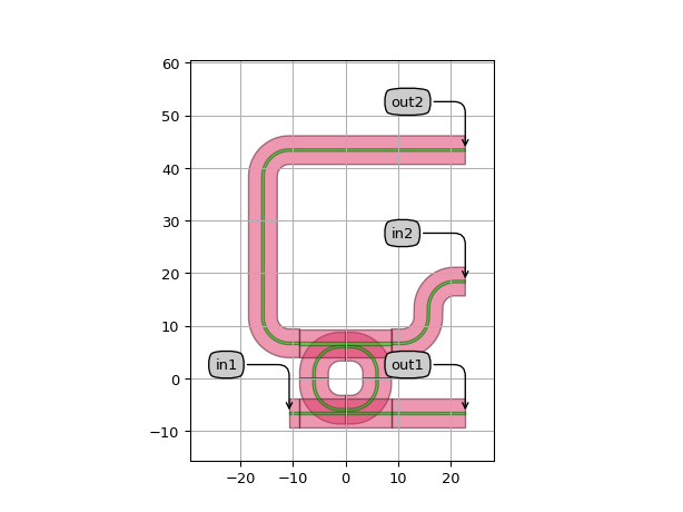
"""The area_layer_on can be used to disable the
drawing of the area between the layers.
"""
import si_fab.all as pdk  # noqa: F401
from picazzo3.filters.ring import RingRect180DropFilter
from picazzo3.container.route_ports import RoutePortsEastWest

my_ring = RingRect180DropFilter()

my_ring_ew = RoutePortsEastWest(
    contents=my_ring,
    east_port_labels=["E0", "E1", "W1"],  # ports to be routed eastwards
    west_port_labels=["W0"],  # ports to be routed westward
)
layout = my_ring_ew.Layout(area_layer_on=False)
layout.visualize(annotate=True)

"""The target_coordinate_east, target_coordinate_west parameters
can be used to specify where the routes should align"""

import si_fab.all as pdk  # noqa: F401
from picazzo3.filters.ring import RingRect180DropFilter
from picazzo3.container.route_ports import RoutePortsEastWest

my_ring = RingRect180DropFilter()

my_ring_ew = RoutePortsEastWest(
    contents=my_ring,
    east_port_labels=["E0", "E1", "W1"],  # ports to be routed eastwards
    west_port_labels=["W0"],  # ports to be routed westward
)
layout = my_ring_ew.Layout(target_coordinate_east=-30.0, target_coordinate_west=30.0)
layout.visualize(annotate=True)

RoutePortsAroundCorner
- class picazzo3.container.route_ports.RoutePortsAroundCorner
Routes ports around a corner of the component in a given direction.
- Parameters:
- trace_template: ( PCell and _WaveguideTemplate ), *None allowed*
Template for all ports, defaults to TECH.PCELLS.WG.DEFAULT.When set to None, the waveguide templates of the ports will be used.
- auto_transition: ( bool, bool_ or int )
If True, automatically transition all ports of contents to the given trace template. If False, no transitions are applied, which might lead to a discontinuity in the waveguide. Also, if trace_template is None, no transitions are applied.
- port_labels: ( List with type restriction, allowed types: <class ‘str’> ), *None allowed*
Labels of the ports to be processed. Set to None to process all ports.
- external_port_names: str
Dictionary for remapping of the port names of the contents to the external ports
- contents: PCell
the contents of the container: the child cell
- name: String that contains only ISO/IEC 8859-1 (extended ASCII py3) or pure ASCII (py2) characters
The unique name of the pcell
- Other Parameters:
- bundle: ( PCell ), locked, *None allowed*
bundle of waveguides added to the contents, generated based on the supplied waveguides list
- waveguides: List with type restriction, allowed types: <class ‘ipkiss3.pcell.cell.pcell.PCell’>, locked
- trace_templates: List with type restriction, allowed types: <class ‘ipkiss3.pcell.cell.pcell.PCell’>, locked
list of templates to apply to all ports
Views
- class Layout
- Parameters:
- first_step_spacing: float and number > 0
The spacing between the routes ( in the section after the first bend )
- reference_coordinate_first_step: float
The minimum 1D coordinate of the first bend of the routes
- first_step_direction: List with value restriction, allowed values: [C2(0.000000, 1.000000), C2(0.000000, -1.000000), C2(1.000000, 0.000000), C2(-1.000000, 0.000000)]
The direction to take when rounding the corner. By default it is 90 degrees off the output direction
- target_coordinate: ( float ), *None allowed*
The coordinate where the endpoints of the waveguides are aligned. An x-coordinate when routing toEAST or WEST, a y-coordinate when routing to NORTH or SOUTH. When the waveguides extend beyond thetarget coordinate, the value is ignored.
- max_s_bend_angle: float and ]0.0,90.0]
- spacing: float
spacing between adjacent output waveguides
- align_outputs: ( bool, bool_ or int )
If True, all outputs will be aligned to the outermost waveguide end, even if it extends beyond its target coordinate.
- reference_coordinate: ( float ), *None allowed*
The coordinate where the first waveguide will be aligned. An x-coordinate if routed towards NORTH or SOUTH,a y-coordinate when routed towards EAST or WEST. If not specified, the x or y coordinate of the first port is taken.
- output_direction: List with value restriction, allowed values: [C2(1.000000, 0.000000), C2(-1.000000, 0.000000), C2(0.000000, 1.000000), C2(0.000000, -1.000000)]
direction of the output waveguides. Should be EAST, WEST, NORTH or SOUTH
- area_layer_on: ( bool, bool_ or int )
When True, the waveguide area will be covered by i3.Rectangles on all cover layers.
- routes:
routes along which the waveguides will be generated
- contents_transformation: GenericNoDistortTransform
transformation to apply to the contents
- flatten_contents: ( bool, bool_ or int )
if True, it will insert the contents as elements in the layout, rather than as an Instance
- view_name: String that contains only alphanumeric characters from the ASCII set or contains _$. ASCII set is extended on PY3.
The name of the view
- manhattan: ( bool, bool_ or int )
Adds rectangular blocks in the bends to avoid as much as possible non-manhattan angles.
- angle_step: float and number > 0
Angle step for rounding.
- rounding_algorithm:
Rounding algorithm used to generate the bends. Can be circular, spline, ….
- bend_radius: float and number > 0
Bend radius for the auto-generated bends.
- Other Parameters:
- target_coordinates: locked
- max_s_bend_angles: locked
- spacings_from_reference: locked
Examples
import si_fab.all as pdk  # noqa: F401
import ipkiss3.all as i3
from picazzo3.filters.ring import RingRect180DropFilter
from picazzo3.container.route_ports import RoutePortsAroundCorner

def annotate_label(ax, text, pos, **kwargs):
    ax.annotate(
        text, xy=pos, horizontalalignment="center", verticalalignment="center", xytext=pos, **kwargs
    )

def annotate_direction(ax, text, direction=i3.DIRECTION.NORTH, pos=(0.0, 0.0), **kwargs):
    kws = {
        "ha": "center",
        "va": "center",
        "rotation": i3.angle_deg(direction),
        "bbox": {
            "boxstyle": "rarrow,pad=0.3",
            "fc": "white",
        },
        "size": 15,
    }

    kws.update(kwargs)
    return ax.text(pos[0], pos[1], text, **kws)

def annotate_distance(
    ax, text, start=(0.0, 0.0), end=(0.0, 10.0), offset=0.0, offset_direction=i3.DIRECTION.EAST, **kwargs
):
    start = (offset_direction * offset) + start
    end = (offset_direction * offset) + end
    ax.annotate(
        "",
        xy=tuple(start),
        xycoords="data",
        xytext=tuple(end),
        textcoords="data",
        arrowprops={"arrowstyle": "<->"},
    )

    text_pos = tuple((e + s) / 2.0 for e, s in zip(start, end))

    if len(text) > 0:
        ax.annotate(text, xy=text_pos, xytext=text_pos, xycoords="data", textcoords="data")

def annotate_y(ax, y, label="", **kwargs):
    return ax.axhline(y, linestyle="dashed", label=label, **kwargs)

def annotate_x(ax, x, label="", **kwargs):
    return ax.axvline(x, linestyle="dashed", label=label, **kwargs)

def annotate(
    ax,
    output_direction=None,
    size_info=None,
    first_step_direction=None,
    first_step_spacing=None,
    reference_coordinate=None,
    reference_coordinate_first_step=None,
    target_coordinate=None,
    spacing=None,
    ports=None,
):
    annotate_label(ax, "contents", (0.0, 0.0), bbox={"fc": "white", "boxstyle": "round", "ec": "black"})

    legend_handles = []
    legend_labels = []
    if first_step_direction is not None:
        pos = (size_info.west - 10.0, (size_info.south + size_info.north) / 2.0)
        annotate_direction(ax, "first_step_direction", direction=first_step_direction, pos=pos)

    if output_direction is not None:
        pos = ((size_info.west + size_info.east) / 2.0, size_info.south - 5.0)
        annotate_direction(ax, "output_direction", direction=output_direction, pos=pos)

    if reference_coordinate is not None:
        legend_handles.append(annotate_y(ax, reference_coordinate, label="reference_coordinate", c="r"))
        legend_labels.append("reference_coordinate")

    if reference_coordinate_first_step is not None:
        legend_handles.append(
            annotate_x(
                ax, reference_coordinate_first_step, label="reference_coordinate_first_step", c="black"
            )
        )
        legend_labels.append("reference_coordinate_first_step")

    if target_coordinate is not None:
        legend_handles.append(annotate_x(ax, target_coordinate, label="target_coordinate"))
        legend_labels.append("target_coordinate")

    if spacing is not None:
        end = tuple(ports.east_ports[0].position)
        start = tuple(ports.east_ports[1].position)
        annotate_distance(ax, "spacing = {}".format(spacing), start=start, end=end, offset=1.0)

    ax.legend(legend_handles, legend_labels)

def visualize_routearoundports(layout):
    size_info = layout.size_info()
    margin = 15.0
    west_margin, east_margin, south_margin, north_margin = [margin] * 4
    box = (
        size_info.west - west_margin,
        size_info.east + east_margin,
        size_info.south - south_margin,
        size_info.north + north_margin,
    )

    fig = layout.visualize(show=False, box=box, canvas_size=(1000.0, 1000.0))
    ax = fig.get_axes()[-1]
    ax.set_aspect("equal", "datalim")

    annotate(
        ax,
        reference_coordinate=layout.reference_coordinate,
        reference_coordinate_first_step=layout.reference_coordinate_first_step,
        first_step_spacing=layout.first_step_spacing,
        target_coordinate=layout.target_coordinate,
        first_step_direction=layout.first_step_direction,
        spacing=layout.spacing,
        output_direction=layout.output_direction,
        ports=layout.ports,
        size_info=size_info,
    )

    from matplotlib.pyplot import show

    show()

my_ring = RingRect180DropFilter()

my_ring_routed = RoutePortsAroundCorner(contents=my_ring, port_labels=["W1", "W0"])  # ports to be routed

layout = my_ring_routed.Layout(
    first_step_direction=i3.DIRECTION.SOUTH,  # when rounding corner, go this direction first
    output_direction=i3.DIRECTION.EAST,  # final output direction
    target_coordinate=30.0,
    reference_coordinate_first_step=-20.0,
    first_step_spacing=15.0,  # Spacing between the waveguides.
)

visualize_routearoundports(layout)
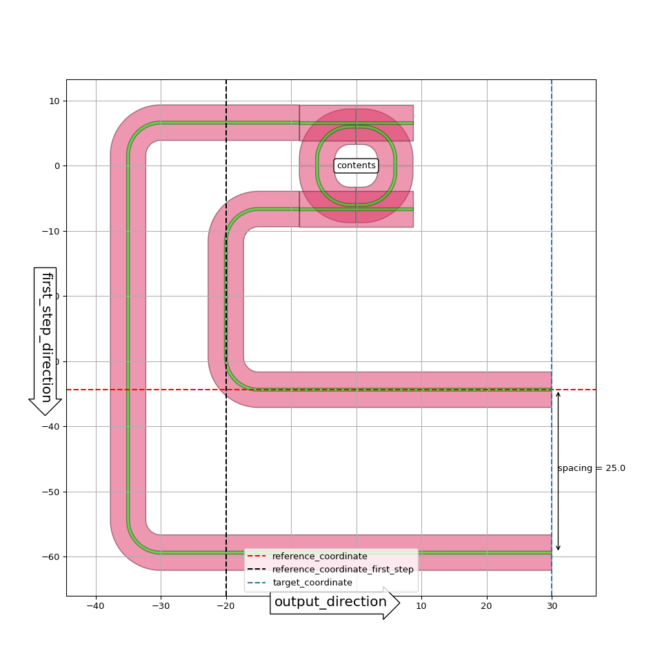
import si_fab.all as pdk  # noqa: F401
import ipkiss3.all as i3
from picazzo3.filters.ring import RingRect180DropFilter
from picazzo3.container.route_ports import RoutePortsAroundCorner

my_ring = RingRect180DropFilter()

my_ring_routed = RoutePortsAroundCorner(contents=my_ring, port_labels=["W1", "W0"])  # ports to be routed

layout = my_ring_routed.Layout(
    first_step_direction=i3.DIRECTION.SOUTH,  # when rounding corner, go this direction first
    output_direction=i3.DIRECTION.EAST,  # final output direction
    first_step_spacing=8.0,  # Spacing between the waveguides.
)
layout.visualize(annotate=True)

"""By default, the area between the routes is drawn,
you can override this using the area_layer_on parameter"""
import si_fab.all as pdk  # noqa: F401
import ipkiss3.all as i3
from picazzo3.filters.ring import RingRect180DropFilter
from picazzo3.container.route_ports import RoutePortsAroundCorner

my_ring = RingRect180DropFilter()

my_ring_routed = RoutePortsAroundCorner(contents=my_ring, port_labels=["W1", "W0"])  # ports to be routed

layout = my_ring_routed.Layout(
    first_step_direction=i3.DIRECTION.SOUTH,  # when rounding corner, go this direction first
    output_direction=i3.DIRECTION.EAST,  # final output direction
    area_layer_on=False,
    first_step_spacing=8.0,  # Spacing between the waveguides.
)
layout.visualize(annotate=True)
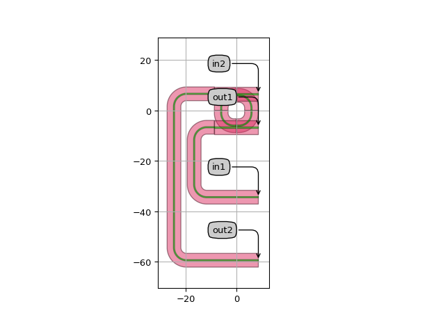
"""Instead of E0, W0, E1, (east 0, west 0 ) ...
we can also use the actual port names as port labels"""
import si_fab.all as pdk  # noqa: F401
import ipkiss3.all as i3
from picazzo3.filters.ring import RingRect180DropFilter
from picazzo3.container.route_ports import RoutePortsAroundCorner

my_ring = RingRect180DropFilter()

my_ring_routed = RoutePortsAroundCorner(contents=my_ring, port_labels=["in1", "out2"])  # ports to be routed

layout = my_ring_routed.Layout(
    first_step_direction=i3.DIRECTION.SOUTH,  # when rounding corner, go this direction first
    output_direction=i3.DIRECTION.EAST,  # final output direction
    first_step_spacing=8.0,  # Spacing between the waveguides.
)
layout.visualize(annotate=True)

"""Be aware that the order of the port_labels is used to determine to the order of the created routes.
If you encounter crossing routes, you might want to change the order of the labels"""
import si_fab.all as pdk  # noqa: F401
import ipkiss3.all as i3
from picazzo3.filters.ring import RingRect180DropFilter
from picazzo3.container.route_ports import RoutePortsAroundCorner

my_ring = RingRect180DropFilter()
layout = my_ring.Layout()

# We first route the E0 (east0 ) port, if we had chosen
# ['W1', 'W0', 'E0'] this would have resulted in crossing waveguides
my_ring = RoutePortsAroundCorner(contents=layout, port_labels=["E0", "W1", "W0"])

layout = my_ring.Layout(
    first_step_direction=i3.DIRECTION.SOUTH,  # when rounding corner, go this direction first
    output_direction=i3.DIRECTION.EAST,  # final output direction
    reference_coordinate_first_step=-20.0,
    first_step_spacing=8.0,  # Spacing between the waveguides.
)
layout.visualize(annotate=True)
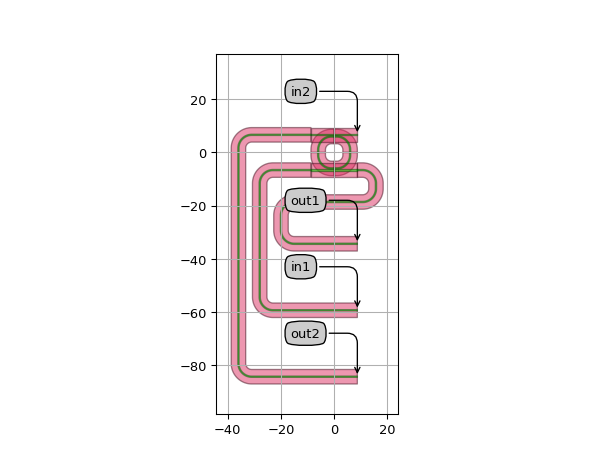
"""As most containers, RoutePortsAroundCorner supports auto transitions.
This means that you can choose a trace template for the routes that's different
from the one used in the contents.
"""
import si_fab.all as pdk  # noqa: F401
import ipkiss3.all as i3
from picazzo3.filters.ring import RingRect180DropFilter
from picazzo3.container.route_ports import RoutePortsAroundCorner
from picazzo3.traces.wire_wg import WireWaveguideTemplate

my_ring = RingRect180DropFilter()
my_ring.Layout()

wtpl = WireWaveguideTemplate()
wtpl.Layout(core_width=0.7)

my_ring = RoutePortsAroundCorner(
    trace_template=wtpl, auto_transition=True, contents=my_ring, port_labels=["E0", "W1", "W0"]
)

layout = my_ring.Layout(
    first_step_direction=i3.DIRECTION.SOUTH,  # when rounding corner, go this direction first
    output_direction=i3.DIRECTION.EAST,  # final output direction
    reference_coordinate_first_step=-20.0,
    target_coordinate=40.0,
    first_step_spacing=8.0,  # Spacing between the waveguides.
)
layout.visualize(annotate=True)
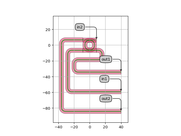
"""The target_coordinate parameter can be used to specify
the 'target coordinate' of the routes. This is illustrated in this example"""

import si_fab.all as pdk  # noqa: F401
import ipkiss3.all as i3
from picazzo3.filters.ring import RingRect180DropFilter
from picazzo3.container.route_ports import RoutePortsAroundCorner

my_ring = RingRect180DropFilter()
layout = my_ring.Layout()

# We first route the E0 (east0 ) port, if we had chosen
# ['W1', 'W0', 'E0'] this would have resulted in crossing waveguides
my_ring = RoutePortsAroundCorner(contents=layout, port_labels=["E0", "W1", "W0"])

layout = my_ring.Layout(
    first_step_direction=i3.DIRECTION.SOUTH,  # when rounding corner, go this direction first
    output_direction=i3.DIRECTION.EAST,  # final output direction
    reference_coordinate_first_step=-20.0,
    target_coordinate=40.0,
    first_step_spacing=8.0,  # Spacing between the waveguides.
)
layout.visualize(annotate=True)
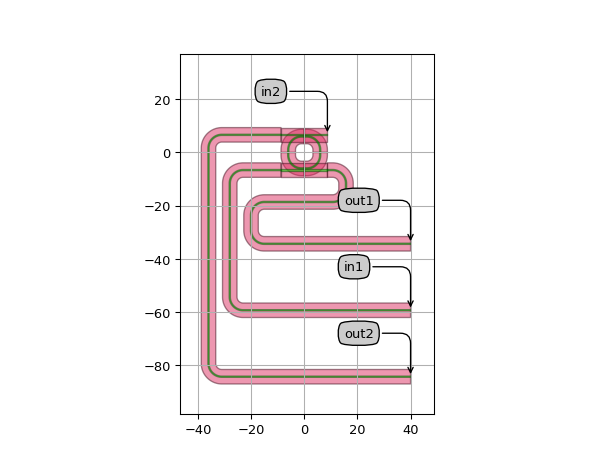
TerminatePorts
TerminatePorts
- class picazzo3.container.terminate_ports.TerminatePorts
Wraps a PCell in a container and terminates the ports specified by the user. If None is given for the port_labels, all ports will be suppressed.
You can also provide another PCell to the property ‘termination’ which will be attached to each terminated port (a stub, to remove reflections). If None is provided, a logical termination is added to the Netlist, but no termination is added in the layout.
- Parameters:
- termination_external_port_name_map: str
dict to map the names of the termination ports that are exposed as external ports. The format is { ‘port_name_on_termination’ : ‘new_name_{port}’ }. The ‘{port}’ in the map will be replaced by the corresponding port name on the component.For instance, when you use grating couplers or detectors as terminations, this map allows you to map the name of the vertical port or the electrical ports to the name of the terminated port on the contents. Similarly, you can use {inst} to insert the name of the instance of the termination. By default, the behavior is ‘{inst}_{port}’.
- termination_port_label: str and String that contains only ISO/IEC 8859-1 (extended ASCII py3) or pure ASCII (py2) characters
label of the port on the termination that will be used to connect to the part of the contents. Default is ‘in’
- termination: PCell
cell which will be used to terminate the ports
- trace_template: ( PCell and _WaveguideTemplate ), *None allowed*
Template for all ports, defaults to TECH.PCELLS.WG.DEFAULT.When set to None, the waveguide templates of the ports will be used.
- termination_instance_prefix: String that contains only alphanumeric characters from the ASCII set or contains _$. ASCII set is extended on PY3.
Prefix for the instance names of the terminations. Default is taken from TECH.CONTAINER.TERMINATE_PORTS
- auto_transition: ( bool, bool_ or int )
If True, automatically transition all ports of contents to the given trace template. If False, no transitions are applied, which might lead to a discontinuity in the waveguide. Also, if trace_template is None, no transitions are applied.
- port_labels: ( List with type restriction, allowed types: <class ‘str’> ), *None allowed*
Labels of the ports to be processed. Set to None to process all ports.
- external_port_names: str
Dictionary for remapping of the port names of the contents to the external ports
- contents: PCell
the contents of the container: the child cell
- name: String that contains only ISO/IEC 8859-1 (extended ASCII py3) or pure ASCII (py2) characters
The unique name of the pcell
- Other Parameters:
- termination_external_port_name_maps: locked
- termination_port_labels: locked
- terminations: List with type restriction, allowed types: <class ‘ipkiss3.pcell.cell.pcell.PCell’>, locked
- trace_templates: List with type restriction, allowed types: <class ‘ipkiss3.pcell.cell.pcell.PCell’>, locked
list of templates to apply to all ports
Examples
"""Layout example of terminated ring resonator"""
import si_fab.all as pdk  # noqa: F401
from picazzo3.filters.ring import RingRect180DropFilter

my_ring = RingRect180DropFilter()
my_ring.Layout()
from picazzo3.container.terminate_ports import TerminatePorts

# Optionally we can add a structure where the ports are suppressed
from picazzo3.apertures.basic import WireWgAperture
from picazzo3.traces.wire_wg import WireWaveguideTemplate

wire_t = WireWaveguideTemplate()
wire_t.Layout(core_width=2.0, cladding_width=6.0)
my_termination = WireWgAperture(name="my_termination", aperture_trace_template=wire_t)
my_termination.Layout(transition_length=4.0)
my_ring_terminated = TerminatePorts(contents=my_ring, port_labels=["E1"], termination=my_termination)
my_ring_terminated_layout = my_ring_terminated.Layout()
my_ring_terminated_layout.visualize(annotate=True)
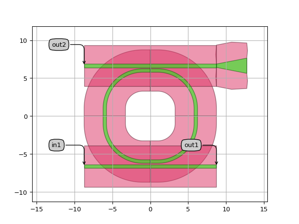
"""Simulation example of terminated ring resonator"""
import si_fab.all as pdk  # noqa: F401
import numpy as np
from picazzo3.filters.ring import RingRect180DropFilter
from picazzo3.container.terminate_ports import TerminatePorts
from picazzo3.logical.termination import Termination
import pylab as plt

my_ring = RingRect180DropFilter()

cp = {
    "cross_coupling1": 1j * 0.05**0.5,  # The coupling from bus to ring and back
    "straight_coupling1": 0.95**0.5,  # Straight coupling
}

my_ring.CircuitModel(ring_length=2 * np.pi * 10.0, coupler_parameters=[cp, cp])

my_termination = Termination()
my_termination.CircuitModel(reflection=0.5**0.5)
my_ring_terminated = TerminatePorts(contents=my_ring, port_labels=["W1"], termination=my_termination)
my_ring_terminated.Netlist()
my_ring_terminated_cm = my_ring_terminated.CircuitModel()

wavelengths = np.linspace(1.535, 1.55, 800)
R = my_ring_terminated_cm.get_smatrix(wavelengths=wavelengths)

plt.figure()
plt.plot(wavelengths, 10 * np.log10(abs(R["in1", "in1"] ** 2)), "r-", label="reflection in1")
plt.plot(wavelengths, 10 * np.log10(abs(R["in1", "out1", :] ** 2)), "b-", label="in port to pass port (out1)")
plt.plot(wavelengths, 10 * np.log10(abs(R["in1", "in2", :] ** 2)), "g-", label="in port to add port (in2)")
plt.xlim([wavelengths[0], wavelengths[-1]])
plt.legend()
plt.show()
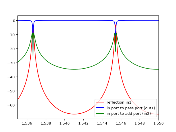
Views
- class Layout
- Parameters:
- termination_transformations: List with type restriction, allowed types: <class ‘ipkiss.geometry.transforms.no_distort.NoDistortTransform’>
Transformations of the terminations. By default, these are calculated to match the ports of the contents.
- contents_transformation: GenericNoDistortTransform
transformation to apply to the contents
- flatten_contents: ( bool, bool_ or int )
if True, it will insert the contents as elements in the layout, rather than as an Instance
- view_name: String that contains only alphanumeric characters from the ASCII set or contains _$. ASCII set is extended on PY3.
The name of the view
Electrical
ContactHole
- class picazzo3.electrical.contact.cell.ContactHole
Regular via to connect M1 (
top_layer) to the silicide layer (bottom_layer) using a contact layer (via_layer)- Parameters:
- name: String that contains only ISO/IEC 8859-1 (extended ASCII py3) or pure ASCII (py2) characters
The unique name of the pcell
Views
- class Layout
A standard electrical via connect M1 (
top_layer) to the silicide layer (bottom_layer) using a contact layer (via_layer).The shape of each layer in the via is a regular polygon with a
n_o_sidessides. and each layer element (top,bottomandvia) is defined through the following properties:top_process
top_purpose
top_width
analogous properties are defined for the other layers.
All those properties can be overridden, but they are defaulting to the values found in TECH.VIAS.CONTACT_HOLE
- Parameters:
- via_width: float and number > 0
Width of the
vialayer (2 * inner radius of the polygon)- via_purpose: PatternPurpose
Purpose of the
vialayer.- via_process: ProcessLayer
Process of the
vialayer.- bottom_width: float and number > 0
Width of the
bottomlayer (2 * inner radius of the polygon)- bottom_purpose: PatternPurpose
Purpose of the
bottomlayer.- bottom_process: ProcessLayer
Process of the
bottomlayer.- top_width: float and number > 0
Width of the
toplayer (2 * inner radius of the polygon)- top_purpose: PatternPurpose
Purpose of the
toplayer.- top_process: ProcessLayer
Process of the
toplayer.- n_o_sides: int and number > 0
Number of sides of the polygon used for the contact hole
- view_name: String that contains only alphanumeric characters from the ASCII set or contains _$. ASCII set is extended on PY3.
The name of the view
- Other Parameters:
- via_shape: locked
- via_layer: locked
- layers: locked
- shapes: locked
- bottom_shape: locked
- bottom_layer: locked
- top_shape: locked
- top_layer: locked
Examples
# Using the default contact hole.
import si_fab.all as pdk  # noqa: F401
from picazzo3.electrical.contact import ContactHole

cell = ContactHole()
layout = cell.Layout()
layout.visualize(annotate=True)
import si_fab.all as pdk  # noqa: F401
from picazzo3.electrical.contact import ContactHole

cell = ContactHole()
layout = cell.Layout(n_o_sides=8, top_width=1.0, bottom_width=0.8, via_width=0.2)
layout.visualize(annotate=True)
Via12
- class picazzo3.electrical.contact.cell.Via12
Regular via to connect M2 (
top_layer) to M1 (bottom_layer) using a contact layer (via_layer)- Parameters:
- name: String that contains only ISO/IEC 8859-1 (extended ASCII py3) or pure ASCII (py2) characters
The unique name of the pcell
Views
- class Layout
A standard electrical via connect M2 (
top_layer) to M1 (bottom_layer) using a contact layer (via_layer).The shape of each layer in the via is a regular polygon with a
n_o_sidessides. and each layer element (top,bottomandvia) is defined through the following properties:top_process
top_purpose
top_width
analogous properties are defined for the other layers.
All those properties can be overridden, but they are defaulting to the values found in TECH.VIAS.VIA12
- Parameters:
- via_width: float and number > 0
Width of the
vialayer (2 * inner radius of the polygon)- via_purpose: PatternPurpose
Purpose of the
vialayer.- via_process: ProcessLayer
Process of the
vialayer.- bottom_width: float and number > 0
Width of the
bottomlayer (2 * inner radius of the polygon)- bottom_purpose: PatternPurpose
Purpose of the
bottomlayer.- bottom_process: ProcessLayer
Process of the
bottomlayer.- top_width: float and number > 0
Width of the
toplayer (2 * inner radius of the polygon)- top_purpose: PatternPurpose
Purpose of the
toplayer.- top_process: ProcessLayer
Process of the
toplayer.- n_o_sides: int and number > 0
Number of sides of the polygon used for the contact hole
- view_name: String that contains only alphanumeric characters from the ASCII set or contains _$. ASCII set is extended on PY3.
The name of the view
- Other Parameters:
- via_shape: locked
- via_layer: locked
- layers: locked
- shapes: locked
- bottom_shape: locked
- bottom_layer: locked
- top_shape: locked
- top_layer: locked
Examples
# Using the default contact hole.
import si_fab.all as pdk  # noqa: F401
from picazzo3.electrical.contact import Via12

cell = Via12()
layout = cell.Layout()
layout.visualize(annotate=True)
import si_fab.all as pdk  # noqa: F401
from picazzo3.electrical.contact import Via12

cell = Via12()
layout = cell.Layout(n_o_sides=8, top_width=1.0, bottom_width=0.8, via_width=0.2)
layout.visualize(annotate=True)
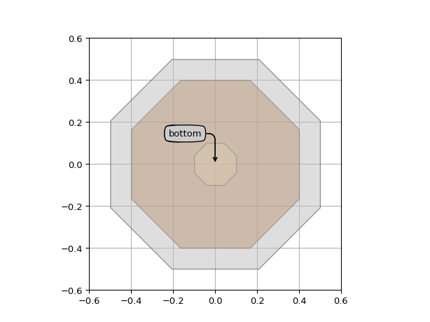
Modulators
Phase Modulators
PhaseShifterWaveguideTemplate
- class picazzo3.modulators.phase.trace.PhaseShifterWaveguideTemplate
Generic phase shifter waveguide trace template. When extruded into a (straight) waveguide, this template draws the necessary implant, contact and metallization layers on top of the underlying waveguide template. This waveguide template should be specified in the “trace_template” property.
This PCell can be used for several types of phase shifters, for example: * P(I)N junction injection or depletion phase shifters, with P and N implants, contacts and metal on two sides * Thermal phase shifters using a metal heater on top * Thermal phase shifters using an implanted waveguide
At the Layout level, windows can be specified separately for the implants (the silicon level), contacts (pre-metal/contact level) and the metallization (e.g. metal1 level). Just fill or leave open each of the three sets of windows, and use them to implement the desired type of phase shifter.
Subclass this PCell to create specialized phase shifters, and add electrical ports.
- Parameters:
- trace_template: PCell and _TraceTemplate
Refers to the other trace template from which information is taken to build this trace template.
- name: String that contains only ISO/IEC 8859-1 (extended ASCII py3) or pure ASCII (py2) characters
The unique name of the pcell
Views
- class Layout
- Parameters:
- metal_windows: List with type restriction, allowed types: <class ‘ipkiss3.pcell.trace.window.window._TraceWindow’>
List of Trace Windows for the metallization layers
- contact_windows: List with type restriction, allowed types: <class ‘ipkiss3.pcell.trace.window.window._TraceWindow’>
List of Trace Windows for the contacts
- implant_windows: List with type restriction, allowed types: <class ‘ipkiss3.pcell.trace.window.window._TraceWindow’>
List of Trace Windows for the implant layers
- windows_for_ports: List with type restriction, allowed types: <class ‘ipkiss3.pcell.trace.window.window._TraceWindow’>
List of Trace Windows from which ports will be generated
- core_width: float and number > 0
width of the waveguide core
- core_layer: __Layer__
layer used to define the core of the waveguide
- flatten_contents: ( bool, bool_ or int )
if True, it will insert the referred trace as elements in the layout, rather than as an Instance
- pin_shape: Shape
shape to be used for the pins
- trace_template_for_ports: _TraceTemplate.Layout
Trace template to be used for the ports. Default = this template
- windows: List with type restriction, allowed types: <class ‘ipkiss3.pcell.trace.window.window._TraceWindow’>
List of Trace Windows to draw on top of the already defined TraceTemplate
- keep_original_trace_template: ( bool, bool_ or int )
- width: float and Real, number and number >= 0
- control_shape_layer: __Layer__
layer on which the control shape is drawn
- draw_control_shape: ( bool, bool_ or int )
draws the control shape on top of the waveguide
- cover_layers: List with type restriction, allowed types: <class ‘ipkiss.primitives.layer.Layer’>
layers that can be used to generate additional coverage of the trace (e.g. manhattan corners)
- view_name: String that contains only alphanumeric characters from the ASCII set or contains _$. ASCII set is extended on PY3.
The name of the view
Examples
import si_fab.all as pdk  # noqa: F401
import ipkiss3.all as i3
from picazzo3.modulators.phase import PhaseShifterWaveguideTemplate
from picazzo3.traces.rib_wg import RibWaveguideTemplate
from picazzo3.electrical.contact import ContactHole

wire_t = RibWaveguideTemplate()
wire_t.Layout(core_width=0.9, cladding_width=2 * i3.TECH.WG.TRENCH_WIDTH + 0.9)

c = ContactHole(name="PNPS_CONT")
c.Layout()

contact_windows = [
    i3.PeriodicArrayReferenceTraceWindow(
        reference=c, offset=-4.0 - 2.5 * i, exclude_ends=(0.5 * 3.0, 0.5 * 3.0), pitch=3.0
    )
    for i in range(3)
]

contact_windows += [
    i3.PeriodicArrayReferenceTraceWindow(
        reference=c, offset=4.0 + 2.5 * i, exclude_ends=(0.5 * 3.0, 0.5 * 3.0), pitch=3.0
    )
    for i in range(3)
]

implant_windows = [
    i3.PathTraceWindow(layer=i3.TECH.PPLAYER.P, start_offset=0.0, end_offset=10.0),
    i3.PathTraceWindow(layer=i3.TECH.PPLAYER.N, start_offset=0.0, end_offset=-10.0),
]

metal_windows = [
    i3.PathTraceWindow(layer=i3.TECH.PPLAYER.M1, start_offset=3.0, end_offset=12.0),
    i3.PathTraceWindow(layer=i3.TECH.PPLAYER.M1, start_offset=-3.0, end_offset=-12.0),
]

ps_t = PhaseShifterWaveguideTemplate(trace_template=wire_t)
ps_t.Layout(contact_windows=contact_windows, implant_windows=implant_windows, metal_windows=metal_windows)

ps = ps_t(name="TestPhaseShifterWaveguideTemplate1")
ps_lay = ps.Layout(shape=[(0.0, 0.0), (50.0, 0.0)])
ps_lay.visualize(annotate=True)
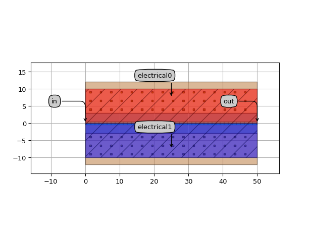
import si_fab.all as pdk  # noqa: F401
import ipkiss3.all as i3
from picazzo3.modulators.phase import PhaseShifterWaveguideTemplate
from picazzo3.traces.rib_wg import RibWaveguideTemplate

wire_t = RibWaveguideTemplate()
wire_t.Layout(core_width=0.9, cladding_width=2 * i3.TECH.WG.TRENCH_WIDTH + 0.9)

metal_windows = [i3.PathTraceWindow(layer=i3.TECH.PPLAYER.M1, start_offset=-1.0, end_offset=1.0)]

ps_t = PhaseShifterWaveguideTemplate(trace_template=wire_t)
ps_t.Layout(metal_windows=metal_windows)

ps = ps_t(name="TestPhaseShifterWaveguideTemplate2")
ps_lay = ps.Layout(shape=[(0.0, 0.0), (50.0, 0.0)])
ps_lay.visualize(annotate=True)
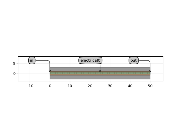
LateralPNPhaseShifterTemplate
- class picazzo3.modulators.phase.trace.LateralPNPhaseShifterTemplate
PN or PIN junction phase shifter with a lateral junction. This is the most ‘classical’ type of phase shifter.
- Parameters:
- n_contact: PCell
- p_contact: PCell
- trace_template: PCell and _TraceTemplate
Refers to the other trace template from which information is taken to build this trace template.
- name: String that contains only ISO/IEC 8859-1 (extended ASCII py3) or pure ASCII (py2) characters
The unique name of the pcell
Views
- class Layout
- Parameters:
- n_bridge_pitch: float
pitch of the N-to-NPLUS bridge, longitudinal direction
- n_bridge_width: float
width of the N-to-NPLUS bridge, longitudinal direction. Set equal to the pitch size to obtain a continuous area.
- p_bridge_pitch: float
pitch of the P-to-PPLUS bridge, longitudinal direction
- p_bridge_width: float
width of the P-to-PPLUS bridge, longitudinal direction. Set equal to the pitch size to obtain a continuous area.
- junction_offset: float
offset of center of junction from the center of the waveguide
- n_metal1_width: float
width of metal1 in the lateral direction, N side
- n_metal1_offset: float
offset of metal1 in the lateral direction, N side
- p_metal1_width: float
width of metal1 in the lateral direction, P side
- p_metal1_offset: float
offset of metal1 in the lateral direction, P side
- n_contact_offsets: list<number > 0>
offsets of the contact plugs in the lateral direction, N side
- n_contact_pitch: float and number > 0
pitch of the contact plugs, longitudinal direction, N side
- p_contact_offsets: list<number > 0>
offsets of the contact plugs in the lateral direction, P side
- p_contact_pitch: float and number > 0
pitch of the contact plugs, longitudinal direction, P side
- n_silicide_extension: float
extension of the silicide area from the trace in longitudinal direction, N side
- n_silicide_width: float
width of the silicide area, in lateral direction, N side
- n_silicide_offset: float
offset of the silicide area from the centerline in lateral direction, N side
- p_silicide_extension: float
extension of the silicide area from the trace in longitudinal direction, P side
- p_silicide_width: float
width of the silicide area, in lateral direction, P side
- p_silicide_offset: float
offset of the silicide area from the centerline in lateral direction, P side
- nplus_extension: float
extension of the P++ area from the trace in longitudinal direction
- nplus_width: float
width of the N++ area, in lateral direction
- nplus_offset: float
offset of the N++ area from the centerline in lateral direction
- n_width: float and Real, number and number >= 0
width of the N+ area, in lateral direction
- pplus_extension: float
extension of the P++ area from the trace in longitudinal direction
- pplus_width: float
width of the P++ area, in lateral direction
- pplus_offset: float
offset of the P++ area from the centerline in lateral direction
- p_width: float and Real, number and number >= 0
width of the P+ area, in lateral direction
- nplus_purpose: PatternPurpose
N++ drawing purpose
- n_purpose: PatternPurpose
N+ drawing purpose
- pplus_purpose: PatternPurpose
P++ drawing purpose
- p_purpose: PatternPurpose
P+ drawing purpose
- metal1_purpose: PatternPurpose
metal1 drawing purpose
- silicide_purpose: PatternPurpose
silicide drawing purpose
- nplus_process: ProcessLayer
N++ implant process, in the contacted area
- n_process: ProcessLayer
N+ implant process (junction)
- pplus_process: ProcessLayer
P++ implant process, in the contacted area
- p_process: ProcessLayer
P+ implant process (junction)
- metal1_process: ProcessLayer
metal1 process
- silicide_process: ProcessLayer
silicide process, in th contacted area
- flipped: ( bool, bool_ or int )
flips P and N side
- junction_overlap: float
overlap of P and N regions. Set to a negative value to obtain a PIN junction
- metal_windows: List with type restriction, allowed types: <class ‘ipkiss3.pcell.trace.window.window._TraceWindow’>
List of Trace Windows for the metallization layers
- contact_windows: List with type restriction, allowed types: <class ‘ipkiss3.pcell.trace.window.window._TraceWindow’>
List of Trace Windows for the contacts
- implant_windows: List with type restriction, allowed types: <class ‘ipkiss3.pcell.trace.window.window._TraceWindow’>
List of Trace Windows for the implant layers
- windows_for_ports: List with type restriction, allowed types: <class ‘ipkiss3.pcell.trace.window.window._TraceWindow’>
List of Trace Windows from which ports will be generated
- core_width: float and number > 0
width of the waveguide core
- core_layer: __Layer__
layer used to define the core of the waveguide
- flatten_contents: ( bool, bool_ or int )
if True, it will insert the referred trace as elements in the layout, rather than as an Instance
- pin_shape: Shape
shape to be used for the pins
- trace_template_for_ports: _TraceTemplate.Layout
Trace template to be used for the ports. Default = this template
- windows: List with type restriction, allowed types: <class ‘ipkiss3.pcell.trace.window.window._TraceWindow’>
List of Trace Windows to draw on top of the already defined TraceTemplate
- keep_original_trace_template: ( bool, bool_ or int )
- width: float and Real, number and number >= 0
- control_shape_layer: __Layer__
layer on which the control shape is drawn
- draw_control_shape: ( bool, bool_ or int )
draws the control shape on top of the waveguide
- cover_layers: List with type restriction, allowed types: <class ‘ipkiss.primitives.layer.Layer’>
layers that can be used to generate additional coverage of the trace (e.g. manhattan corners)
- view_name: String that contains only alphanumeric characters from the ASCII set or contains _$. ASCII set is extended on PY3.
The name of the view
Examples
"""PN phase shifter"""
import si_fab.all as pdk  # noqa: F401
import ipkiss3.all as i3
from picazzo3.modulators.phase import LateralPNPhaseShifterTemplate
from picazzo3.traces.rib_wg import RibWaveguideTemplate
from picazzo3.electrical.contact import ContactHole

wire_t = RibWaveguideTemplate()
wire_t.Layout(core_width=0.9, cladding_width=2 * i3.TECH.WG.TRENCH_WIDTH + 0.9)

c = ContactHole(name="LPNPS_CONT")

ps_t = LateralPNPhaseShifterTemplate(trace_template=wire_t, p_contact=c, n_contact=c)

ps = ps_t(name="ExampleLateralPNPhaseShifterTemplate")
ps_lay = ps.Layout(shape=[(0.0, 0.0), (10.0, 0.0)])
ps_lay.visualize(annotate=True)
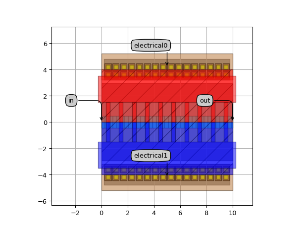
"""PN phase shifter with continuous P-PPLUS/N-NPLUS bridges"""
import si_fab.all as pdk  # noqa: F401
import ipkiss3.all as i3
from picazzo3.modulators.phase import LateralPNPhaseShifterTemplate
from picazzo3.traces.rib_wg import RibWaveguideTemplate
from picazzo3.electrical.contact import ContactHole

wire_t = RibWaveguideTemplate()
wire_t.Layout(core_width=0.9, cladding_width=2 * i3.TECH.WG.TRENCH_WIDTH + 0.9)

c = ContactHole(name="LPNPS2_CONT")

ps_t = LateralPNPhaseShifterTemplate(trace_template=wire_t, p_contact=c, n_contact=c)

ps_t.Layout(p_bridge_pitch=1.0, p_bridge_width=1.0, n_bridge_pitch=1.0, n_bridge_width=1.0)

ps = ps_t(name="ExampleLateralPNPhaseShifterTemplate2")
ps_lay = ps.Layout(shape=[(0.0, 0.0), (10.0, 0.0)])

ps_lay.visualize(annotate=True)

"""PN phase shifter with offset junction and overlapping P and N"""
import si_fab.all as pdk  # noqa: F401
import ipkiss3.all as i3
from picazzo3.modulators.phase import LateralPNPhaseShifterTemplate
from picazzo3.traces.rib_wg import RibWaveguideTemplate
from picazzo3.electrical.contact import ContactHole

wire_t = RibWaveguideTemplate()
wire_t.Layout(core_width=0.9, cladding_width=2 * i3.TECH.WG.TRENCH_WIDTH + 0.9)

c = ContactHole(name="LPNPS3_CONT")

ps_t = LateralPNPhaseShifterTemplate(trace_template=wire_t, p_contact=c, n_contact=c)
ps_t.Layout(
    p_bridge_pitch=1.0,
    p_bridge_width=0.6,
    n_bridge_pitch=1.0,
    n_bridge_width=0.6,
    junction_offset=0.2,
    junction_overlap=0.1,
)

ps = ps_t(name="ExampleLateralPNPhaseShifterTemplate3")
ps_lay = ps.Layout(shape=[(0.0, 0.0), (10.0, 0.0)])

ps_lay.visualize(annotate=True)
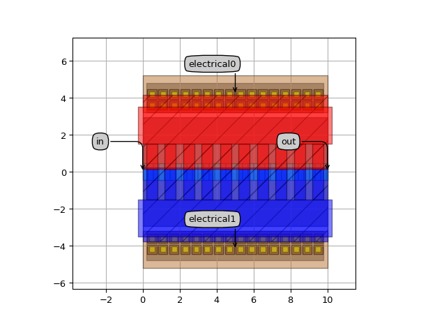
"""PN phase shifter with flipped P and N side"""
import si_fab.all as pdk  # noqa: F401
import ipkiss3.all as i3
from picazzo3.modulators.phase import LateralPNPhaseShifterTemplate
from picazzo3.traces.rib_wg import RibWaveguideTemplate
from picazzo3.electrical.contact import ContactHole

wire_t = RibWaveguideTemplate()
wire_t.Layout(core_width=0.9, cladding_width=2 * i3.TECH.WG.TRENCH_WIDTH + 0.9)

c = ContactHole(name="LPNPSF_CONT")

ps_t = LateralPNPhaseShifterTemplate(trace_template=wire_t, p_contact=c, n_contact=c)

ps_t.Layout(
    p_bridge_pitch=1.0,
    p_bridge_width=0.6,
    n_bridge_pitch=1.0,
    n_bridge_width=0.6,
    junction_offset=0.2,
    junction_overlap=0.1,
    flipped=True,
)

ps = ps_t(name="ExampleLateralPNPhaseShifterTemplateFlipped")
ps_lay = ps.Layout(shape=[(0.0, 0.0), (10.0, 0.0)])
ps_lay.visualize(annotate=True)
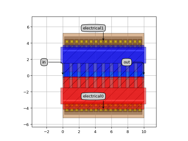
"""PIN phase shifter"""
import si_fab.all as pdk  # noqa: F401
import ipkiss3.all as i3
from picazzo3.modulators.phase import LateralPNPhaseShifterTemplate
from picazzo3.traces.rib_wg import RibWaveguideTemplate
from picazzo3.electrical.contact import ContactHole

wire_t = RibWaveguideTemplate()
wire_t.Layout(core_width=0.9, cladding_width=2 * i3.TECH.WG.TRENCH_WIDTH + 0.9)

c = ContactHole(name="LPINPS_CONT")

ps_t = LateralPNPhaseShifterTemplate(trace_template=wire_t, p_contact=c, n_contact=c)
ps_t.Layout(
    p_bridge_pitch=1.0, p_bridge_width=0.6, n_bridge_pitch=1.0, n_bridge_width=0.6, junction_overlap=-0.15
)

ps = ps_t(name="ExampleLateralPINPhaseShifterTemplate")
ps_lay = ps.Layout(shape=[(0.0, 0.0), (10.0, 0.0)])
ps_lay.visualize(annotate=True)

LongitudinalPNPhaseShifterTemplate
- class picazzo3.modulators.phase.trace.LongitudinalPNPhaseShifterTemplate
PN or PIN junction phase shifter with a longitudinal (interdigited) junction.
- Parameters:
- n_contact: PCell
- p_contact: PCell
- trace_template: PCell and _TraceTemplate
Refers to the other trace template from which information is taken to build this trace template.
- name: String that contains only ISO/IEC 8859-1 (extended ASCII py3) or pure ASCII (py2) characters
The unique name of the pcell
Views
- class Layout
- Parameters:
- n_length: float and Real, number and number >= 0
length of the N+ area, in longitudinal direction (finger width)
- p_length: float and Real, number and number >= 0
length of the P+ area, in longitudinal direction (finger width)
- n_metal1_width: float
width of metal1 in the lateral direction, N side
- n_metal1_offset: float
offset of metal1 in the lateral direction, N side
- p_metal1_width: float
width of metal1 in the lateral direction, P side
- p_metal1_offset: float
offset of metal1 in the lateral direction, P side
- n_contact_offsets: list<number > 0>
offsets of the contact plugs in the lateral direction, N side
- n_contact_pitch: float and number > 0
pitch of the contact plugs, longitudinal direction, N side
- p_contact_offsets: list<number > 0>
offsets of the contact plugs in the lateral direction, P side
- p_contact_pitch: float and number > 0
pitch of the contact plugs, longitudinal direction, P side
- n_silicide_extension: float
extension of the silicide area from the trace in longitudinal direction, N side
- n_silicide_width: float
width of the silicide area, in lateral direction, N side
- n_silicide_offset: float
offset of the silicide area from the centerline in lateral direction, N side
- p_silicide_extension: float
extension of the silicide area from the trace in longitudinal direction, P side
- p_silicide_width: float
width of the silicide area, in lateral direction, P side
- p_silicide_offset: float
offset of the silicide area from the centerline in lateral direction, P side
- nplus_extension: float
extension of the P++ area from the trace in longitudinal direction
- nplus_width: float
width of the N++ area, in lateral direction
- nplus_offset: float
offset of the N++ area from the centerline in lateral direction
- n_width: float and Real, number and number >= 0
width of the N+ area, in lateral direction
- pplus_extension: float
extension of the P++ area from the trace in longitudinal direction
- pplus_width: float
width of the P++ area, in lateral direction
- pplus_offset: float
offset of the P++ area from the centerline in lateral direction
- p_width: float and Real, number and number >= 0
width of the P+ area, in lateral direction
- nplus_purpose: PatternPurpose
N++ drawing purpose
- n_purpose: PatternPurpose
N+ drawing purpose
- pplus_purpose: PatternPurpose
P++ drawing purpose
- p_purpose: PatternPurpose
P+ drawing purpose
- metal1_purpose: PatternPurpose
metal1 drawing purpose
- silicide_purpose: PatternPurpose
silicide drawing purpose
- nplus_process: ProcessLayer
N++ implant process, in the contacted area
- n_process: ProcessLayer
N+ implant process (junction)
- pplus_process: ProcessLayer
P++ implant process, in the contacted area
- p_process: ProcessLayer
P+ implant process (junction)
- metal1_process: ProcessLayer
metal1 process
- silicide_process: ProcessLayer
silicide process, in th contacted area
- flipped: ( bool, bool_ or int )
flips P and N side
- junction_overlap: float
overlap of P and N regions. Set to a negative value to obtain a PIN junction
- metal_windows: List with type restriction, allowed types: <class ‘ipkiss3.pcell.trace.window.window._TraceWindow’>
List of Trace Windows for the metallization layers
- contact_windows: List with type restriction, allowed types: <class ‘ipkiss3.pcell.trace.window.window._TraceWindow’>
List of Trace Windows for the contacts
- implant_windows: List with type restriction, allowed types: <class ‘ipkiss3.pcell.trace.window.window._TraceWindow’>
List of Trace Windows for the implant layers
- windows_for_ports: List with type restriction, allowed types: <class ‘ipkiss3.pcell.trace.window.window._TraceWindow’>
List of Trace Windows from which ports will be generated
- core_width: float and number > 0
width of the waveguide core
- core_layer: __Layer__
layer used to define the core of the waveguide
- flatten_contents: ( bool, bool_ or int )
if True, it will insert the referred trace as elements in the layout, rather than as an Instance
- pin_shape: Shape
shape to be used for the pins
- trace_template_for_ports: _TraceTemplate.Layout
Trace template to be used for the ports. Default = this template
- windows: List with type restriction, allowed types: <class ‘ipkiss3.pcell.trace.window.window._TraceWindow’>
List of Trace Windows to draw on top of the already defined TraceTemplate
- keep_original_trace_template: ( bool, bool_ or int )
- width: float and Real, number and number >= 0
- control_shape_layer: __Layer__
layer on which the control shape is drawn
- draw_control_shape: ( bool, bool_ or int )
draws the control shape on top of the waveguide
- cover_layers: List with type restriction, allowed types: <class ‘ipkiss.primitives.layer.Layer’>
layers that can be used to generate additional coverage of the trace (e.g. manhattan corners)
- view_name: String that contains only alphanumeric characters from the ASCII set or contains _$. ASCII set is extended on PY3.
The name of the view
Examples
import si_fab.all as pdk  # noqa: F401
import ipkiss3.all as i3
from picazzo3.modulators.phase import LongitudinalPNPhaseShifterTemplate
from picazzo3.traces.rib_wg import RibWaveguideTemplate
from picazzo3.electrical.contact import ContactHole

wire_t = RibWaveguideTemplate()
wire_t.Layout(core_width=0.9, cladding_width=2 * i3.TECH.WG.TRENCH_WIDTH + 0.9)

c = ContactHole(name="LPINPS_CONT")

ps_t = LongitudinalPNPhaseShifterTemplate(trace_template=wire_t, p_contact=c, n_contact=c)
ps_t.Layout(p_length=0.3, n_length=0.5, junction_overlap=0.05)

ps = ps_t(name="ExampleLongitundinalPNPhaseShifterTemplate")
ps_lay = ps.Layout(shape=[(0.0, 0.0), (10.0, 0.0)])
ps_lay.visualize(annotate=True)
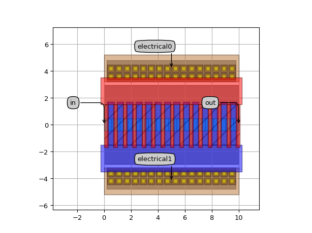
PhaseModulator
- class picazzo3.modulators.phase.cell.PhaseModulator
Straight Phase Modulator PCell. Takes a trace template for the modulator, generates a phase modulator waveguide and adds transitions. Exposes the optical and electrical ports and terms of the (tapered) phase modulator waveguide.
Make sure to explicitly specify the ports to be tapered (the optical ports) in port_labels. Specify the length of the modulator in the Layout View.
- Parameters:
- contents: PCell
the contents of the container: the child cell
- trace_template: ( PCell and _WaveguideTemplate ), *None allowed*
Template for all ports, defaults to TECH.PCELLS.WG.DEFAULT.When set to None, the waveguide templates of the ports will be used.
- transition_database: AutoTransitionDatabase
AutoTransitionDatabase in which the correct transition between the two trace templates can be looked up.
- transitions: List with type restriction, allowed types: <class ‘ipkiss3.pcell.cell.pcell.PCell’>
Transitions (of type WaveguideTransitionFromPort) attached the the ports given in port_labels. Should be in the same order as port_labels.
- port_labels: ( List with type restriction, allowed types: <class ‘str’> ), *None allowed*
Labels of the ports to be processed. Set to None to process all ports.
- external_port_names: str
Dictionary for remapping of the port names of the contents to the external ports
- modulator_trace_template: PCell and _TraceTemplate and PhaseShifterWaveguideTemplate
trace template to use for the phase modulator waveguide
- name: String that contains only ISO/IEC 8859-1 (extended ASCII py3) or pure ASCII (py2) characters
The unique name of the pcell
- Other Parameters:
- trace_templates: List with type restriction, allowed types: <class ‘ipkiss3.pcell.cell.pcell.PCell’>, locked
list of templates to apply to all ports
Views
- class Layout
- Parameters:
- flatten_contents: ( bool, bool_ or int )
if True, it will insert the contents as elements in the layout, rather than as an Instance
- transition_length: ( float and Real, number and number >= 0 ), *None allowed*
Length of the transition. Set to None to take the standard transition length.
- zero_length_if_identical: ( bool, bool_ or int )
uses a zero-length transition if the trace templates are identical
- flatten_transitions: ( bool, bool_ or int )
if true, flattens the transitions one level
- straight_extension: ( Coord2 and number >= 0 ), *None allowed*
Tuple: straight extensions of the transitions. Set to None to take the standard straight extensions
- contents_transformation: GenericNoDistortTransform
transformation to apply to the contents
- length: float and Real, number and number >= 0
length of the phase modulator waveguide
- view_name: String that contains only alphanumeric characters from the ASCII set or contains _$. ASCII set is extended on PY3.
The name of the view
- Other Parameters:
- transition_lengths: locked
Examples
import si_fab.all as pdk  # noqa: F401
import ipkiss3.all as i3
from picazzo3.modulators.phase import LateralPNPhaseShifterTemplate, PhaseModulator
from picazzo3.traces.rib_wg import RibWaveguideTemplate
from picazzo3.electrical.contact import ContactHole

wire_t = RibWaveguideTemplate()
wire_t.Layout(core_width=0.9, cladding_width=2 * i3.TECH.WG.TRENCH_WIDTH + 0.9)
c = ContactHole(name="LPNPS3_CONT")

ps_t = LateralPNPhaseShifterTemplate(trace_template=wire_t, p_contact=c, n_contact=c)
ps_t.Layout(
    p_bridge_pitch=1.0,
    p_bridge_width=0.6,
    n_bridge_pitch=1.0,
    n_bridge_width=0.6,
    junction_offset=0.2,
    junction_overlap=0.1,
)

pmod = PhaseModulator(modulator_trace_template=ps_t, port_labels=["in", "out"])
pmod_lay = pmod.Layout(length=100.0)
pmod_lay.visualize(annotate=True)