ConnectElectrical
- class ipkiss3.all.ConnectElectrical
A connector that uses
i3.RouteManhattanto connect two electrical ports.This connector is supposed to be used together with
i3.Circuitori3.place_and_route.- Parameters:
- end_angle: ( float ), optional, *None allowed*
Angle of the end port of the connector, pointing towards the route
- start_angle: ( float ), optional, *None allowed*
Angle of the start port of the connector, pointing towards the route
- min_spacing: float and Real, number and number >= 0, optional
minimal spacing between parallel sections of the route
- end_straight: float and Real, number and number >= 0, optional
The length of the straight end section of the route
- start_straight: float and Real, number and number >= 0, optional
The length of the straight start section of the route
- min_straight: float and Real, number and number >= 0, optional
The minimum length of any straight sections in the route
- angle_step: float and number > 0, optional
angle step for rounding
- rounding_algorithm: optional
Rounding algorithm (ShapeRound, ShapeRoundAdiabaticSpline, …). Takes a shape as input and returns a new (rounded) shape.
- bend_radius: float and number > 0, optional
bend radius for the auto-generated bends
- control_points: list, optional
Control the routing by passing either a list of points
i3.CPthrough which the route has to pass,or a list ofi3.H/i3.Vinstances.- trace_template: ( PCell and _TraceTemplate ), optional, *None allowed*
Trace template to use for the waveguide between the two ports, when the ports have a different template, transitions will be added. When this property is left unspecified/None the trace_template of the start_port will be used
- Other Parameters:
- cover_layers: locked, *None allowed*
- cover_bends: locked, *None allowed*
- fixed_bend90: locked, *None allowed*
Examples
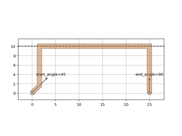
"""
This example illustrates how you can use the `control_points` property to guide
your electrical wire.
"""
import si_fab.all as pdk  # noqa: F401
from picazzo3.electrical.contact import Via12
from ipkiss3 import all as i3
import matplotlib.pyplot as plt

# Placing the components in a circuit
via = Via12()
circuit = i3.Circuit(
    insts={"via_1": via, "via_2": via},
    specs=[
        i3.Place("via_1", position=(0, 0)),
        i3.Place("via_2", position=(25, 0)),
        i3.ConnectElectrical(
            "via_1:top",
            "via_2:top",
            start_angle=45,
            end_angle=90,
            control_points=[i3.H(10)],
        ),
    ],
)
circuit_layout = circuit.Layout()
fig = circuit_layout.visualize(show=False)
ax = fig.axes[0]
ax.annotate(
    "start_angle=45",
    xy=(0, 0),
    xytext=(4, 4),
    va="center",
    ha="center",
    arrowprops=dict(arrowstyle="<-", facecolor="black"),
)
ax.annotate(
    "end_angle=90",
    xy=(25, 0),
    xytext=(25, 4),
    va="center",
    ha="center",
    arrowprops=dict(arrowstyle="<-", facecolor="black"),
)
plt.axhline(10, color="k", linestyle="--")
plt.show()
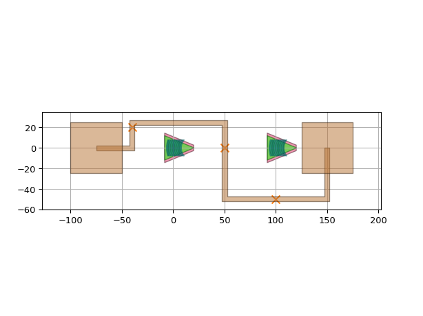
"""
This example illustrates how you can use the `control_points` property to avoid obstacles
"""
import si_fab.all as pdk  # noqa: F401
from picazzo3.fibcoup.curved import FiberCouplerCurvedGrating
from ipkiss3 import all as i3
import matplotlib.pyplot as plt

class BondPad(i3.PCell):
    class Layout(i3.LayoutView):
        size = i3.Size2Property(default=(50.0, 50.0), doc="Size of the bondpad")
        metal_layer = i3.LayerProperty(default=i3.TECH.PPLAYER.M1.LINE, doc="Metal used for the bondpad")

        def _generate_elements(self, elems):
            elems += i3.Rectangle(layer=self.metal_layer, box_size=self.size)
            return elems

        def _generate_ports(self, ports):
            ports += i3.ElectricalPort(
                name="m1",
                position=(0.0, 0.0),
                shape=i3.ShapeRectangle(box_size=self.size),
                process=self.metal_layer.process,
            )
            return ports

# Placing the components in a circuit
bp = BondPad()
bp_layout = bp.Layout(size=(50, 50))
gr = FiberCouplerCurvedGrating()

control_points = [i3.CP((-40, 20), i3.NORTH), i3.CP((50, 0), i3.SOUTH), i3.CP((100, -50), i3.EAST)]

wire_template = i3.ElectricalWireTemplate()
wire_template.Layout(width=5.0, layer=bp_layout.metal_layer)

circuit = i3.Circuit(
    insts={"gr": gr, "gr2": gr, "b1": bp, "b2": bp},
    specs=[
        i3.Place("gr", position=(0, 0)),
        i3.Place("gr2", position=(100, 0)),
        i3.Place("b1", position=(-75, 0)),
        i3.Place("b2", position=(+150, 0)),
        i3.ConnectElectrical(
            "b1:m1",
            "b2:m1",
            start_angle=0.0,
            end_angle=-90.0,
            control_points=control_points,
            rounding_algorithm=None,
            trace_template=wire_template,
        ),
    ],
)

circuit_layout = circuit.Layout()
circuit_layout.visualize(show=False)
plt.scatter([cp[0] for cp in control_points], [cp[1] for cp in control_points], c="C1", s=80, marker="x")
plt.show()
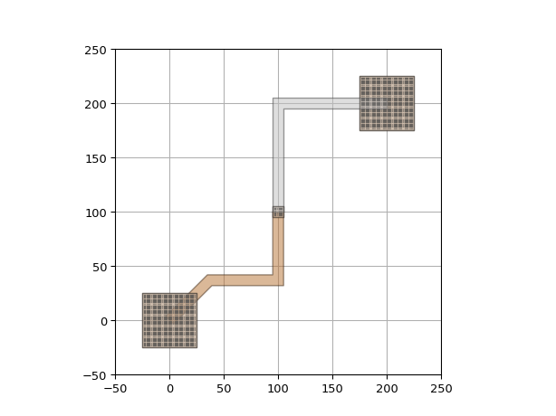
"""
This example illustrates how you can use the `trace_template` property
to change trace template of your electrical wire
"""
import si_fab.all as pdk  # noqa: F401
import ipkiss3.all as i3

bp = pdk.BondPad()
M1_wire_tpl = pdk.M1WireTemplate().Layout(width=10)

circuit = i3.Circuit(
    insts={"pad1": bp, "pad2": bp},
    specs=[
        i3.Place("pad1", (0, 0)),
        i3.Place("pad2", (150, 150)),
        i3.ConnectElectrical(
            "pad1:m1",
            "pad2:m1",
            trace_template=M1_wire_tpl,
            start_angle=0,
            end_angle=180,
            control_points=[i3.V(100)],
        ),
    ],
)
circuit.get_default_view(i3.LayoutView).visualize()
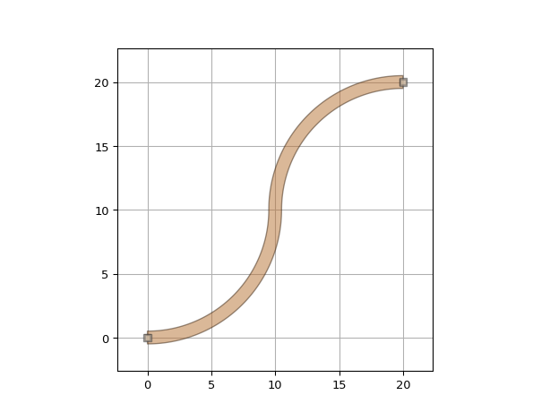
import si_fab.all as pdk  # noqa
import ipkiss3.all as i3
from picazzo3.electrical.contact import Via12

via = Via12()

circuit = i3.Circuit(
    insts={"via1": via, "via2": via},
    specs=[
        i3.Place("via1", (0, 0)),
        i3.Place("via2", (20, 20)),
        i3.ConnectElectrical(
            "via1:top",
            "via2:top",
            start_angle=0,
            end_angle=180,
            bend_radius=10,
            rounding_algorithm=i3.ShapeRound,
            min_straight=0,
        ),
    ],
)
circuit.Layout().visualize(annotate=True)
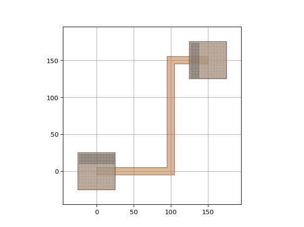
"""
This example illustrates how you can use `i3.VIA` to implement multi-layer electrical connection
"""
import si_fab.all as pdk  # noqa
import ipkiss3.all as i3

class VIA_M1_M2_ARRAY(i3.PCell):
    box_size = i3.Size2Property(default=(10, 10))
    via_pitch = i3.Size2Property(
        default=i3.TECH.BONDPAD.VIA_PITCH, doc="2D pitch (center-to-center) of the vias"
    )
    via = i3.ChildCellProperty(doc="Via used")

    def _default_via(self):
        return pdk.VIA_M1_M2()

    class Layout(i3.LayoutView):
        def _generate_elements(self, elems):
            elems += i3.Rectangle(layer=i3.TECH.PPLAYER.M1, box_size=self.box_size)
            elems += i3.Rectangle(layer=i3.TECH.PPLAYER.M2, box_size=self.box_size)
            return elems

        def _generate_instances(self, insts):
            periods_x = int(self.box_size[0] / self.via_pitch[0]) - 1
            periods_y = int(self.box_size[1] / self.via_pitch[1]) - 1

            insts += i3.ARef(
                reference=self.via,
                origin=(
                    -(periods_x - 1) * self.via_pitch[0] / 2.0,
                    -(periods_y - 1) * self.via_pitch[1] / 2.0,
                ),
                period=self.via_pitch,
                n_o_periods=(periods_x, periods_y),
            )
            return insts

bp = pdk.BondPad()
via_array = VIA_M1_M2_ARRAY()
M1_wire_tpl = pdk.M1WireTemplate().Layout(width=10)
M2_wire_tpl = pdk.M2WireTemplate().Layout(width=10)

circuit = i3.Circuit(
    insts={"pad1": bp, "pad2": bp},
    specs=[
        i3.Place("pad1", (0, 0)),
        i3.Place("pad2", (200, 200)),
        i3.ConnectElectrical(
            "pad1:m1",
            "pad2:m2",
            start_angle=45,
            start_straight=50,
            end_angle=180,
            trace_template=M1_wire_tpl,
            control_points=[
                i3.VIA(
                    (100, 100),
                    direction_in=i3.SOUTH,
                    direction_out=i3.NORTH,
                    trace_template=M2_wire_tpl,  # change end trace template
                    layout=via_array,
                ),
            ],
        ),
    ],
)

circuit.Layout().visualize()