Release notes Luceda Photonics Design Platform 3.10.0
Luceda 3.10 is a major release featuring many improvements and new functionalities to our design platform. Notably, it marks the introduction of IPKISS Canvas, which is available to all IPKISS users without requiring any additional licenses.
In addition, there are many other highlights in this release:
Our netlist extraction now also extracts electrical nets, with the ability to extract multilayer nets through VIAs.
IPKISS is now significantly faster, building upon the performance enhancements from our previous releases.
There is a new drawing primitive for functionally describing shapes.
There is a dedicated connector for drawing electrical connections.
For a comprehensive list of new features, improvements and bugfixes, please consult the changelog.
Introducing IPKISS Canvas
We are proud to present to you IPKISS Canvas, which is a completely new Graphical User Interface (GUI) that interacts with IPKISS. IPKISS Canvas allows you to explore and verify existing IPKISS designs that are generated through Python code in a schematic view. You can also use it to intuitively create new PIC designs in a matter of minutes. At the same time, code remains at the center of the IPKISS experience, as the expressiveness and precision of code are crucial in building complex PICs.
Canvas acts as a copilot by providing an alternative way to look at your PIC circuits - from a schematic perspective. This assists in creating and modifying your circuits throughout the design process leading up to tape-out. It helps discover, review, and adjust critical parts of your PICs, from important information about your PDK and design parameters, to connectivity and annotation of important parameters.
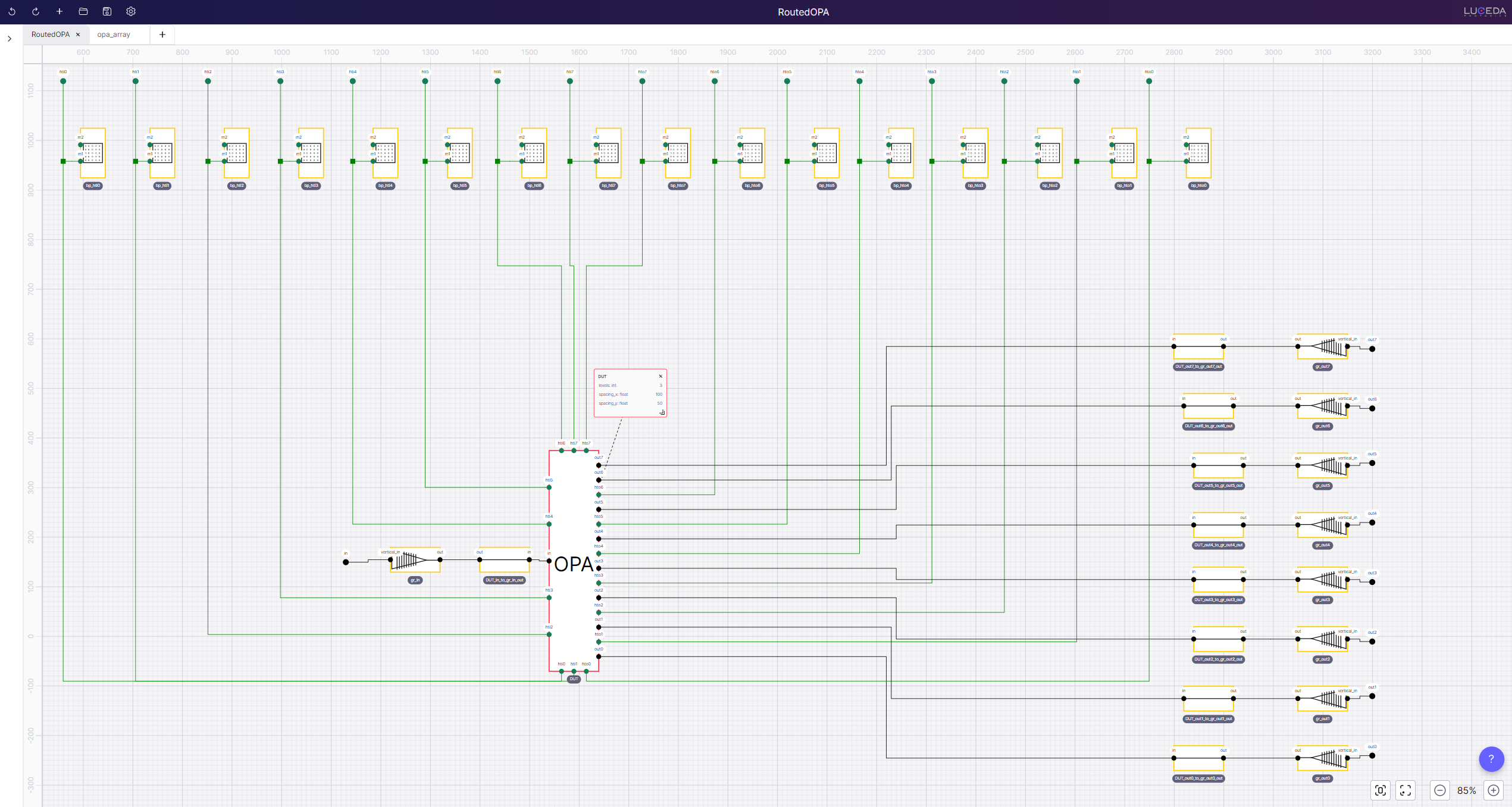
Schematic of an optical phased array in IPKISS Canvas.
IPKISS Canvas offers a wide range of functionalities:
Functional verification: check design connectivity, parameters of your PCells, and annotate layouts with critical information, such as waveguide lengths.
Communication: share your in-progress designs, containing the most relevant and up-to-date information, with colleagues.
Boosting productivity: streamline your workflow by browsing through libraries and PDKs. Discover what a component looks like, easily find port names to implement circuit connectivity, and obtain tips about the Python code needed to achieve specific functionality.
Schematic capture: quickly develop your PIC designs from scratch in a schematic environment, then transition these schematics into code, while avoiding any implementation mistakes through our code generation capabilities or direct design loading in IPKISS.
Additional resources
Luceda Academy tutorial: Introduction to IPKISS Canvas for schematic capture.
Luceda Academy example: Example of an Optical phased array.
Netlist extraction: support for electrical nets
IPKISS 3.10 introduces new advanced netlist extraction capabilities. In previous versions, it was possible to extract the optical netlist and overlapping electrical ports, such as exposed ports. With IPKISS 3.10, we have expanded this functionality to include the extraction of connections between electrical ports of instances. This provides the ability to extract the complete electrical netlist based on the physical implementation, including transitions between metal layers through VIAs.
When your designs are exported to IPKISS Canvas using to_canvas, both optical and electrical connectivity will be extracted.
Please note that the behavior of i3.NetlistFromLayout has not changed: it still extracts optical connectivity and exposed electrical ports, but it does not include electrical nets between instances.
In terms of the schematic visualized in IPKISS Canvas, this means the following:
Optical waveguides are shown as waveguide cells, each with their own annotations, such as waveguide length.
Electrical traces (both DC/RF) are shown as nets.
For a complete insight, check i3.NetlistExtractionSettings to further explore how the netlist extraction can be used for design verification.
Performance
IPKISS has been made faster in various areas of the platform. The startup time for importing IPKISS and PDKs has been notably reduced, and numerous aspects of layout generation have been improved, enhancing the code run time across the whole Luceda Photonics Design Platform. In addition, layout visualization using Matplotlib is now several order of magnitudes faster! This improvement applies both when running scripts directly and when using Jupyter notebooks.
Parametric shapes
IPKISS 3.10 introduces a new drawing primitive for creating parametric shapes, by specifying a function curve(t) -> x(t), y(t).
You can check i3.ParametricShape for documentation and examples.
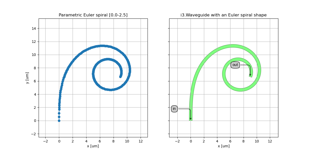
Euler spiral parametric curve and a waveguide shaped based on it.
Based on the parametric shape, three specialized curves are defined, e.g. the raised sine, cosine and radial s-bends. See S-bend Shapes.
Electrical connector
As part of our ongoing efforts to enhance our place and route engine, we have introduced a new electrical connector in this release: i3.ConnectElectrical.
This connector allows to connect two electrical ports and can be used within the i3.Circuit and i3.place_and_route framework.
Compared to the optical Manhattan connector, the electrical connector doesn’t round by default (but a rounding algorithm can still be provided if rounding is needed), and allows to start/finish the route at arbitrary angles.
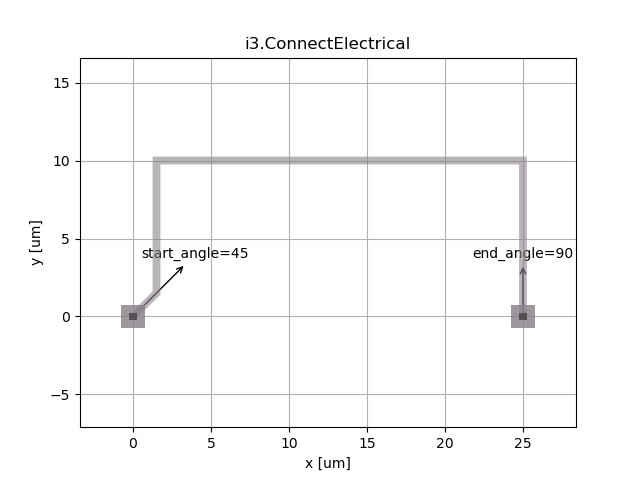
Electrical connector connecting two BondPads.