Designing a multimode interferometer (MMI)
PCells and Views
To design a component in IPKISS, it is important to understand the concept of a PCell. A PCell is the blueprint for creating a component in IPKISS. It contains all of the information about it.
In IPKISS, PCells are represented by a Python class.
The components themselves are therefore objects created from that class.
To create your own PCells, you need to inherit from i3.PCell.
To illustrate, let’s take the example of an MMI.
We first begin by choosing a name for our MMI PCell that describes what it is.
Since it’s a 1-by-2 MMI, we call it MMI1x2.
We then define a class with this name and inherit from i3.PCell using the code below.
We also provide a docstring to explain what it does.
class MMI1x2(i3.PCell):  # we define a component using i3.PCell
    """MMI with 1 input and 2 outputs."""  # a short description of the class is always useful to include
PCells in IPKISS have what are known as views that describe different aspects of a component. These views are implemented as inner classes of a PCell, that is, as a class that belongs to another class.
For example, the LayoutView describes the layout of a component.
A PCell can also have other views that describe its interconnectivity or how it is simulated (which will be explained in later tutorials).
class Layout(i3.LayoutView):
Creating an MMI layout
Inside this inner class, you describe how to create the layout of the PCell you are designing.
The simplest way to do this, for a PCell without any subcells, is to use _generate_elements.
This is a method of LayoutView that returns what are known as elements.
These are shapes drawn on a particular layer and are used as the geometrical building blocks of a layout.
Let’s take a look at the example below for an MMI:
        def _generate_elements(self, elems):
            # 2. We are using "TECH.PPLAYER.SI" as the layer for the elements. This is defined in the PDK technology
            # files and refers to a specific process layer in the foundry. We will look at layers in more depth later.

            elems += i3.Rectangle(  # we use "i3.Rectangle()" to create the main body of the MMI
                layer=pdk.TECH.PPLAYER.SI,
                center=(10, 0.0),
                box_size=(20, 6),
            )
            elems += i3.Wedge(  # we use "i3.Wedge()" to create the input and output tapers
                layer=pdk.TECH.PPLAYER.SI,
                begin_coord=(-5, 0.0),
                end_coord=(0.0, 0.0),
                begin_width=0.45,
                end_width=1,
            )
            elems += i3.Wedge(
                layer=pdk.TECH.PPLAYER.SI,
                begin_coord=(20, 1),
                end_coord=(25, 1),
                begin_width=1,
                end_width=0.45,
            )
            elems += i3.Wedge(
                layer=pdk.TECH.PPLAYER.SI,
                begin_coord=(20, -1),
                end_coord=(25, -1),
                begin_width=1,
                end_width=0.45,
            )
            return elems
In this example, we use two different kinds of elements: i3.Rectangle to create the multimode waveguide section of the MMI and i3.Wedge to create the input and output tapers.
Other element classes exist to create different shapes.
You can find a complete list of elements in Elements and Layers.
Note that some elements, that are references to the layout of another PCell, should instead be added to _generate_instances (see Creating a Basic Layout for an explanation of how to do that).
To these elements, you need to provide geometrical parameters such as the center and box_size parameter of i3.Rectangle.
You need to also provide the layer on which the element is to be drawn to the layer parameter.
These layers are defined in the technology of a PDK and their names vary based on the PDK in question.
In this case we use the SI layer in our example PDK SiFab and so refer to it as pdk.TECH.PPLAYER.SI.
Putting it all together, and we have a PCell that looks like the following:
class MMI1x2(i3.PCell):  # we define a component using i3.PCell
    """MMI with 1 input and 2 outputs."""  # a short description of the class is always useful to include

    class Layout(i3.LayoutView):
        # 1. The _generate_elements(self, elems) returns a list called elems, which contains all the elements in our
        # component. An element is simply a shape/polygon on a layer. Here we add a few elements using some basic
        # IPKISS pre-defined shapes. You can also add a generic polygon if you can't find the shape you need.

        def _generate_elements(self, elems):
            # 2. We are using "TECH.PPLAYER.SI" as the layer for the elements. This is defined in the PDK technology
            # files and refers to a specific process layer in the foundry. We will look at layers in more depth later.

            elems += i3.Rectangle(  # we use "i3.Rectangle()" to create the main body of the MMI
                layer=pdk.TECH.PPLAYER.SI,
                center=(10, 0.0),
                box_size=(20, 6),
            )
            elems += i3.Wedge(  # we use "i3.Wedge()" to create the input and output tapers
                layer=pdk.TECH.PPLAYER.SI,
                begin_coord=(-5, 0.0),
                end_coord=(0.0, 0.0),
                begin_width=0.45,
                end_width=1,
            )
            elems += i3.Wedge(
                layer=pdk.TECH.PPLAYER.SI,
                begin_coord=(20, 1),
                end_coord=(25, 1),
                begin_width=1,
                end_width=0.45,
            )
            elems += i3.Wedge(
                layer=pdk.TECH.PPLAYER.SI,
                begin_coord=(20, -1),
                end_coord=(25, -1),
                begin_width=1,
                end_width=0.45,
            )
            return elems
This is a PCell for an MMI with particular layout.
Instantiating and visualizing an MMI layout
Instantiating the MMI can be done by simply using the following code:
default_mmi = MMI1x2()
Then, you can instantiate its layout with
default_mmi_layout = default_mmi.Layout()
From the layout object, you can obtain a lot of information.
Firstly, you can visualize it using the visualize method of the LayoutView:
default_mmi_layout.visualize(annotate=True)
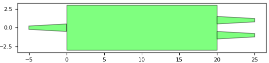
Default MMI layout visualization
You can write it to a GDS using write_gdsii to see what it will look like in the GDS file you will submit for tapeout:
default_mmi_layout.write_gdsii("mmi_layout.gds")
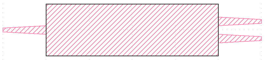
Default MMI layout GDS
You can create a topview of the component with information on the material stacks using visualize_2d:
default_mmi_layout.visualize_2d(process_flow=pdk.TECH.VFABRICATION.PROCESS_FLOW_FEOL)
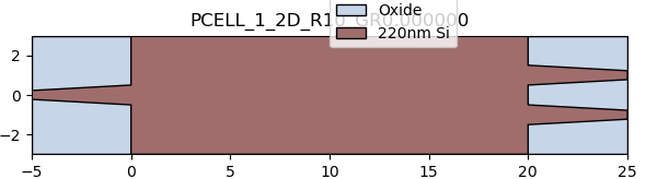
Default MMI layout 2D visualization with material stacks
And you can take a look at its cross-section by using the cross_section method and then visualizing it:
default_mmi_layout.cross_section(
     cross_section_path=i3.Shape([(-0.5, -1.5), (-0.5, 1.5)]),
     process_flow=pdk.TECH.VFABRICATION.PROCESS_FLOW_FEOL,
 ).visualize()
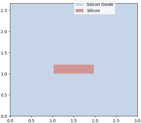
Default MMI cross section
In both of these cases, the 3D geometry of the component is assembled first in what is known as a virtual fabrication process defined in the PDK. You can provide the virtual fabrication process you want to use to the parameter ‘process_flow’.
Adding ports to your MMI
To use your MMI in a circuit, you need to define ports for it. This will allow you to connect your components together when you define your circuit as explained in Designing a splitter tree.
These are defined inside of a method called _generate_ports.
Much like for _generate_elements, you should override this method in the LayoutView of your PCell.
In this case, it should return a list of ports that your PCell will have.
In the case of a 1x2 MMI, it has three optical ports: one input and two outputs.
We define them using i3.OpticalPort and a set of variables, such as the port name, its position and angle.
        def _generate_ports(self, ports):
            trace_template = self.trace_template

            ports += i3.OpticalPort(  # you can also add electrical ports in the same way
                name="in1",  # this is the port name you will see when this PCell is used
                position=(-5, 0.0),  # position is coincident with the relevant element
                angle=180.0,  # angle with respect to the x-axis, always facing outwards from the port
                trace_template=trace_template,  # the trace template for the optical port
            )
            ports += i3.OpticalPort(
                name="out1",
                position=(25, -1),
                angle=0.0,
                trace_template=trace_template,
            )
            ports += i3.OpticalPort(
                name="out2",
                position=(25, 1),
                angle=0.0,
                trace_template=trace_template,
            )
            return ports
If we were to add electrical ports, we would be defining them using i3.ElectricalPort but the underlying concepts are the same.
Each optical port requires something called a trace template. This describes the waveguide “cross-section” at the port. It is a type of class that describes all the information needed to create a waveguide, for example it contains which layers the waveguide will be drawn in and the width of these layers. From this you can determine the cross-section. It can also include simulation data such its effective indices, or instructions for creating more elaborate layouts, but this will not be covered in this tutorial. By providing a trace template as a parameter to a port, you can explain what type of waveguide it is compatible with.
Making your MMI parametric to a trace template
In our case, we are creating a 1x2 MMI.
We notice that the information from a trace template can be used to obtain other information for the layout.
For example, we can use the waveguide core layer to define the layers for the MMI structures.
This ensures the waveguide and MMI structures are always in the same layer, without having to hard code the layer, making the PCell more generic.
The layer for the waveguide cladding (the cladding_layer) can be used for a cladding around the MMI.
Finally, the width of the waveguide core (the core_width) can be obtained from the trace template to provide the width of the ends of the tapers of the MMI.
Doing so is not only useful, but also ensures the waveguide and MMI will share the same dimensions, eliminating the possibility of a discontinuity.
To this end, we update our _generate_elements method to obtain these values from the trace template and add an additional cladding for our MMI:
        def _generate_elements(self, elems):
            # 2. We directly use the process layers from the trace template to define the layers for the entire
            # structure, as we want the MMI to use the same layers as the input and output waveguides. The waveguide
            # width is also used to set the taper width to ensure they are matched to the waveguides.

            core_layer = self.trace_template.core_layer
            core_width = self.trace_template.core_width
            cladding_layer = self.trace_template.cladding_layer

            elems += i3.Rectangle(  # we use "i3.Rectangle()" to create the main body of the mmi
                layer=core_layer,
                center=(10, 0.0),
                box_size=(20, 6),
            )
            elems += i3.Wedge(  # we use "i3.Wedge()" to create the input and output tapers
                layer=core_layer,
                begin_coord=(-5, 0.0),
                end_coord=(0.0, 0.0),
                begin_width=core_width,
                end_width=1,
            )
            elems += i3.Wedge(
                layer=core_layer,
                begin_coord=(20, 1),
                end_coord=(25, 1),
                begin_width=1,
                end_width=core_width,
            )
            elems += i3.Wedge(
                layer=core_layer,
                begin_coord=(20, -1),
                end_coord=(25, -1),
                begin_width=1,
                end_width=core_width,
            )

            elems += i3.Rectangle(  # we can add a cladding layer as well to improve performance
                layer=cladding_layer,
                center=(10, 0.0),
                box_size=(32, 8),
            )
            return elems

        # 3. Finally, we add some optical ports to our design. These are a virtual addition to the design, which will
        # not appear in the final GDS file, but are used by IPKISS as a common language between component and circuit
        # layout, as well as during simulations. We have seen how optical ports can be used to connect and place
        # instances in the circuit section. A port needs to have a domain (electrical or optical), unique name, a
        # position, an angle and trace template.
        #
        # When connecting ports with different trace templates, IPKISS will use a trace template transition (e.g. a
        # taper between materials or widths) if one is available in the PDK.
Now, we need to get the trace template from somewhere. We define it in our PCell at the level of properties. This is where you define all the different parameters of your cell that you can vary.
Let’s take a brief look at the properties:
class MMI1x2(i3.PCell):
    """MMI with 1 input and 2 outputs."""

    # 1. Here we define an MMI PCell in the same way as before, but with a trace template property. This is a template
    # for a type of waveguide from the PDK. We can then access these properties to ensure our device is compatible with
    # the waveguides that connect with it.

    _name_prefix = "MMI1x2"  # this name will be the prefix in every instance of this class
    trace_template = i3.TraceTemplateProperty(doc="Trace template of the access waveguide.")

    def _default_trace_template(self):  # this trace template is defined in the PDK
        return pdk.SiWireWaveguideTemplate()
We provide in our properties a value to _name_prefix.
This will be used as a prefix to the name of each cell in your layout.
In our example, we have the following:
_name_prefix = "MMI1x2"
which means each MMI in our circuit layout will be called MMI1x2_1, MMI1x2_2, MMI1x2_3, etc.
Then, we define the property for the trace template. Using the following code:
trace_template = i3.TraceTemplateProperty(doc="Trace template of the access waveguide.")
we give this property the name of trace_template and use i3.TraceTemplateProperty to restrict it to only to inputs that are a trace template.
This is something that we recommend you do, as it makes it clear how your PCell is being used.
We then provide a default value to the trace template.
To do so, we define a method with the name _default_trace_template which means that IPKISS will take the value returned by this method and use it as the default value of trace_template.
In our case, we have the following code which returns the class SiWireWaveguideTemplate from SiFab and uses it as the trace template for the MMI ports.
def _default_trace_template(self):  # this trace template is defined in the PDK
      return pdk.SiWireWaveguideTemplate()
Now, when we visualize our layout, we can see its ports:
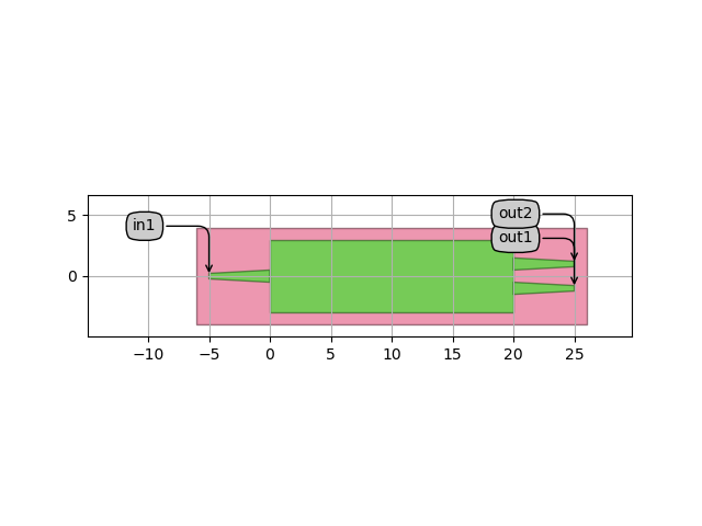
Use .visualize(annotate=True) to visualize a layout with its ports
Making your MMI fully parametric
Following the same principle, you can make your MMI parametric to other properties too.
For example, rather than hard-coding the geometrical properties of your MMI, you can define them as parameters that you can vary.
You would need to define descriptive, understandable names for these parameters.
In our case, we choose the names width, length, taper_width, taper_length and waveguide_spacing as these describe what these parameters represent.
Since they are all positive quantities, we restrict them to positive numerical values by defining them as instances of i3.PositiveNumberProperty.
We then provide default values to the default parameter of i3.PositiveNumberProperty and an explanation what they represent to its doc parameter.
The properties of our MMI now look like this:
class MMI1x2(i3.PCell):
    """MMI with 1 input and 2 outputs."""

    # 1. Creating parameters is exactly the same for an i3.PCell as it is for an i3.Circuit. We have added the
    # trace_template parameter with a default method.

    _name_prefix = "MMI1x2"  # adding a name that will be added to every instance of this class
    trace_template = i3.TraceTemplateProperty(doc="Trace template of the access waveguide.")
    width = i3.PositiveNumberProperty(default=4.0, doc="Width of the MMI section.")
    length = i3.PositiveNumberProperty(default=20.0, doc="Length of the MMI section.")
    taper_width = i3.PositiveNumberProperty(default=1.0, doc="Width of the taper.")
    taper_length = i3.PositiveNumberProperty(default=5.0, doc="Length of the taper.")
    waveguide_spacing = i3.PositiveNumberProperty(default=2.0, doc="Spacing between the waveguides.")

    def _default_trace_template(self):
        return pdk.SiWireWaveguideTemplate()
We can then remove hard-coded values from _generate_elements and _generate_ports and instead have them refer to parameters:
        def _generate_elements(self, elems):
            # 2. Similar to the circuit, here we are creating some local variables to improve the readability of
            # the code.

            length = self.length
            width = self.width
            taper_length = self.taper_length
            taper_width = self.taper_width
            half_waveguide_spacing = 0.5 * self.waveguide_spacing
            core_layer = self.trace_template.core_layer
            cladding_layer = self.trace_template.cladding_layer
            core_width = self.trace_template.core_width

            # Si core
            elems += i3.Rectangle(
                layer=core_layer,
                center=(0.5 * length, 0.0),
                box_size=(length, width),
            )
            elems += i3.Wedge(
                layer=core_layer,
                begin_coord=(-taper_length, 0.0),
                end_coord=(0.0, 0.0),
                begin_width=core_width,
                end_width=taper_width,
            )
            elems += i3.Wedge(
                layer=core_layer,
                begin_coord=(length, half_waveguide_spacing),
                end_coord=(length + taper_length, half_waveguide_spacing),
                begin_width=taper_width,
                end_width=core_width,
            )
            elems += i3.Wedge(
                layer=core_layer,
                begin_coord=(length, -half_waveguide_spacing),
                end_coord=(length + taper_length, -half_waveguide_spacing),
                begin_width=taper_width,
                end_width=core_width,
            )

            # Cladding
            elems += i3.Rectangle(
                layer=cladding_layer,
                center=(0.5 * length, 0.0),
                box_size=(length + 2 * taper_length, width + 2.0),
            )
            return elems
Now, we have an MMI that is ready for use!
Parametrizing the number of inputs and output
We can go even further and make the number of inputs and outputs of our MMI parametric. By using for loops, you can loop over each input and output and create tapers and ports for them. You can see below what code for that MMI could look like. We won’t go into more detail about its actual implementation.
class MMI(i3.PCell):
    _name_prefix = "MMI"
    trace_template = i3.TraceTemplateProperty(doc="Trace template of the access waveguide.")
    width = i3.PositiveNumberProperty(default=4.0, doc="Width of the MMI section.")
    length = i3.PositiveNumberProperty(default=20.0, doc="Length of the MMI secion.")
    taper_width = i3.PositiveNumberProperty(default=1.0, doc="Width of the taper.")
    taper_length = i3.PositiveNumberProperty(default=5.0, doc="Length of the taper.")
    waveguide_spacing = i3.PositiveNumberProperty(default=2.0, doc="Spacing between the waveguides.")
    n_inputs = i3.PositiveIntProperty(default=1, doc="The number of inputs for the MMI")
    n_outputs = i3.PositiveIntProperty(default=2, doc="The number of outputs for the MMI")

    # 1. We have added the number of inputs and outputs as parameters, allowing us to call this class to create any
    # nxm MMI.

    def _default_trace_template(self):
        return pdk.SiWireWaveguideTemplate()

    def validate_properties(self):
        # 2. The width of the MMI needs to be large enough for the input/output ports to be placed with the desired
        # spacing. We want to keep the width independent of these parameters, so instead of linking these parameters we
        # use the "validate_properties" method to check that the design is physical. If the parameters are set in such
        # a way that a sensible design is not possible, this function will raise an error with a description of the
        # problem.

        wg_number = max(self.n_inputs, self.n_outputs)  # find the largest number of waveguide connections
        if self.width < (wg_number - 1) * self.waveguide_spacing + self.taper_width:
            raise i3.PropertyValidationError(  # error raised if the above criteria is not met
                self,
                "The sum of waveguide_spacing plus the taper exceeds the width of the MMI",
                {"width": self.width, "waveguide_spacing": self.waveguide_spacing, "taper_width": self.taper_width},
            )
        if self.waveguide_spacing < self.taper_width:
            raise i3.PropertyValidationError(
                self,
                "The waveguides will overlap: waveguide_spacing is too small or width is too big",
                {"taper_width": self.taper_width, "waveguide_spacing": self.waveguide_spacing},
            )
        return True

    class Layout(i3.LayoutView):
        def _generate_elements(self, elems):
            length = self.length
            width = self.width
            taper_length = self.taper_length
            taper_width = self.taper_width
            waveguide_spacing = self.waveguide_spacing
            core_layer = self.trace_template.core_layer
            cladding_layer = self.trace_template.cladding_layer
            waveguide_width = self.trace_template.core_width
            n_inputs = self.n_inputs
            n_outputs = self.n_outputs

            elems += i3.Rectangle(
                layer=core_layer,
                center=(0.5 * length, 0.0),
                box_size=(length, width),
            )

            # 3. Instead of adding each taper separately, we can use a for loop to iterate through each position and add
            # the correct number of tapers. We use two loops, one for the input tapers and one for the output tapers.
            # The "input_start" object is a local variable to simplify placement of the tapers.

            for waveguide in range(n_inputs):
                input_start = (n_inputs - 1) * waveguide_spacing
                elems += i3.Wedge(
                    layer=core_layer,
                    begin_coord=(-taper_length, -input_start / 2 + waveguide * waveguide_spacing),
                    end_coord=(0.0, -input_start / 2 + waveguide * waveguide_spacing),
                    begin_width=waveguide_width,
                    end_width=taper_width,
                )

            for waveguide in range(n_outputs):
                output_start = (n_outputs - 1) * waveguide_spacing
                elems += i3.Wedge(
                    layer=core_layer,
                    begin_coord=(length, -output_start / 2 + waveguide * waveguide_spacing),
                    end_coord=(
                        length + taper_length,
                        -output_start / 2 + waveguide * waveguide_spacing,
                    ),
                    begin_width=taper_width,
                    end_width=waveguide_width,
                )

            # 4. We also add some cladding over the entire device, again using the trace template to define this layer.

            elems += i3.Rectangle(
                layer=cladding_layer,
                center=(0.5 * length, 0.0),
                box_size=(length + 2 * taper_length, width + 2.0),
            )
            return elems

        def _generate_ports(self, ports):  # we place the ports in the same way as the tapers
            length = self.length
            taper_length = self.taper_length
            waveguide_spacing = self.waveguide_spacing
            trace_template = self.trace_template
            n_inputs = self.n_inputs
            n_outputs = self.n_outputs

            for waveguide in range(n_inputs):
                input_start = (n_inputs - 1) * waveguide_spacing
                ports += i3.OpticalPort(
                    name=f"in{waveguide+1}",
                    position=(-taper_length, -input_start / 2 + waveguide * waveguide_spacing),
                    angle=180.0,
                    trace_template=trace_template,
                )
            for waveguide in range(n_outputs):
                output_start = (n_outputs - 1) * waveguide_spacing
                ports += i3.OpticalPort(
                    name=f"out{waveguide+1}",
                    position=(length + taper_length, -output_start / 2 + waveguide * waveguide_spacing),
                    angle=0.0,
                    trace_template=trace_template,
                )
            return ports

    # 5. A netlist for this component can be directly generated from the layout using the class
    # below. A netlist is a set of instances, exposed ports and logical connections that define
    # a component or circuit. You can modify the netlist, or create it from scratch if you prefer.

    class Netlist(i3.NetlistFromLayout):
        pass
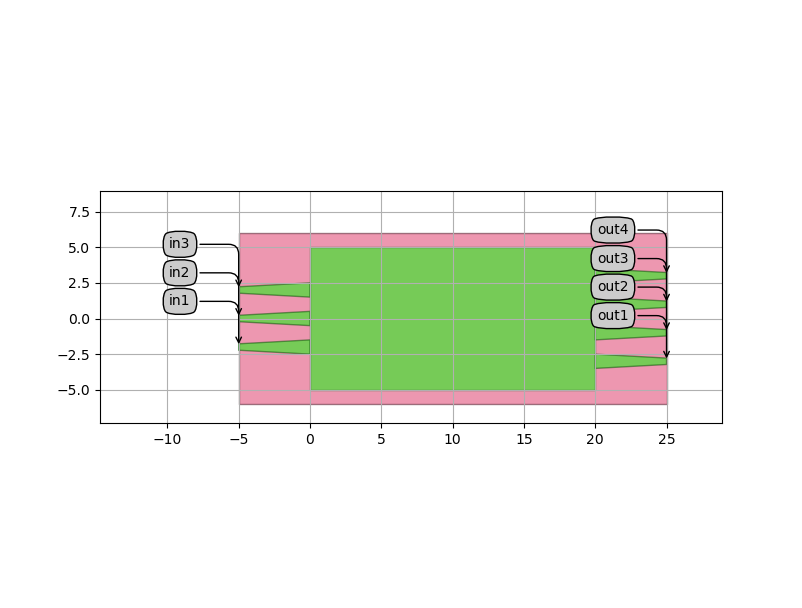
Parametric / generalized MMI with three inputs and four outputs
Note the addition of the method validate_properties.
This is a method that you can use to make sure that the parameters of your MMI lead to a valid layout.
You can make it return True except in those cases in which you know that the layout will be invalid.
In those cases, it will return an exception (i.e. crash) with a customizable error message that explains the problem.
Fixed cells
A useful tool that you can use is the concept of fixed cells. Let’s say that you found a set of parameters for your component in which it is optimized at a certain frequency. You want to easily instantiate your component with that set of parameters. You also want to avoid accidentally providing a different set of parameters.
The solution to this is to create what is known as a fixed cell.
This is a component for which the parameters are frozen and so cannot be set.
To create a fixed cell, you need to add a line that says @i3.lock_properties() just before the start of your PCell.
This line is known as a decorator and instructs IPKISS to lock this class to a certain set of properties.
We provide below an example of how to do that. We will inherit MMI1x2 from the PDK and then lock it with some optimized values for 1550 nm operation.
@i3.lock_properties()
class MMI1x2Optimized1550(pdk.MMI1x2):
    """MMI1x2 with layout parameters optimized for maximum transmission at 1550 nm."""

    data_tag = i3.LockedProperty()  # as with other properties, we add the LockedProperty inside the class

    def _default_data_tag(self):
        return "mmi_1x2_optimized_1550"

    def _default_name(self):
        return self.data_tag.upper()

    def _default_trace_template(self):
        tt = pdk.SiWireWaveguideTemplate(name=self.name + "_tmpl")
        tt.Layout(core_width=0.45)
        return tt

    # 2. Instead of adding properties for all the parameters, we just define the default functions, as it is not
    # possible to change them. The values we hard code here were optimised using Camfr, a built-in 2D EME propagation
    # tool available in IPKISS. If you are interested in component simulation we have numerous options, from the
    # built-in solver, to commercial links with third party software, which streamlines the design process.

    def _default_width(self):
        return 4.0

    def _default_length(self):
        return i3.snap_value(14.0258356928 / 2.0) * 2.0  # Snap to twice the grid size so that the edges are on the grid

    def _default_taper_width(self):
        return i3.snap_value(1.49982527224 / 2.0) * 2.0  # Snap to twice the grid size so that the edges are on the grid

    def _default_taper_length(self):
        return 5.0

    def _default_waveguide_spacing(self):
        return i3.snap_value(2.00712657136 / 2.0) * 2.0  # Snap to twice the grid size so that the edges are on the grid
More information
Exercise
Now that we have learned how to create the layout of a PCell, let’s apply what we learned to a different example.
In the path src/training/getting_started/5_component_layout/2_exercises/exercises.py in the downloaded samples for Luceda Academy, you will find a PCell for a grating coupler that is incomplete.
There are ellipses in various locations in which some code needs to be added.
Could you open that file and add the missing code?