Creating a First Circuit Simulation
With IPKISS, you can run circuit simulations to create a better understanding of the time and frequency behavior of your opto-electronic circuit. These circuit simulations rely on behavioral models for each of the devices in the circuit. A behavioral model allows to simulate the circuit sufficiently fast without loosing too much accuracy. Instead of running a full physical simulation (such as Finite Difference Time Domain or Beam Propagation Method), the device is represented by a more approximate but faster model, such as a set of differential equations or a S-matrix.
Usually, foundry process design kits already contain predefined compact models for the validated devices in the foundry’s library. Both for foundries building their own compact models, and for designers who use their own custom devices or technology, IPKISS allows great flexibility to write your own compact models. This is done in the CircuitModel view of the PCell. Luceda’s circuit simulator, Caphe, can then run simulations in both time and frequency domain, using the model descriptions the user / fab has defined.
In the CircuitModel view you can define compact models and hierarchical models. As explained above, such circuit models declare the behavior of a device, both for frequency-and time dependent behavior. Hierarchical models are used to describe subcircuits. They contain a list of instances that refer to behavioral circuit models of the subcomponents, and how they are connected to each other.
First example of a model
A compact model based on a scattering matrix looks like this:
class MyModel(i3.CompactModel):
    def calculate_smatrix(parameters, env, S):
        S['port1', 'port2'] = ...
The calculate_smatrix has three arguments:
parameters: this is an object that contains all parameters that are defined on the model. Later we will see how to define them.
env: this is the environment. It contains variables that are globally defined, such as the wavelength, frequency (c/wavelength), temperature. Currently this object only holds the wavelength variables, but this can be extended by the user defining the simulation.
S: the S-matrix. You can set the S-matrix elements using
S[port_name1, port_name2] = .... See also scatter matrix intro for a mathematical intro to S-matrices.
Inside calculate_smatrix, you define the transmission from/to each port in the device.
Below is an example for an optical waveguide, which has a phase delay that depends on the length and effective index of the device:
class MyModel(i3.CompactModel):
    parameters = [
      'n_eff',
      'length'
    ]

    terms = [
      i3.OpticalTerm(name='in'),
      i3.OpticalTerm(name='out'),
    ]

    def calculate_smatrix(parameters, env, S):
        phase = 2 * np.pi / env.wavelength * parameters.n_eff * parameters.length
        A = 0.99
        S['in', 'out'] = S['out', 'in'] = A * np.exp(1j * phase)
To assign this model to a PCell, IPKISS defines the CircuitModelView. In the next paragraph we explain the anatomy of the CircuitModel view.
Note
The S-matrix is by default initialized at zero. That means you don’t have to write each element in the S-matrix explicitly. So in the example above, we do not need to write S[‘in’, ‘in’] = S[‘out’, ‘out’] = 0.
Defining the CircuitModel view
A circuit model in IPKISS is defined inside the i3.CircuitModelView of a PCell.
Here’s how it is written:
class MyPCell(i3.PCell):

    class CircuitModel(i3.CircuitModelView):
        param1 = i3.PositiveNumberProperty(doc="Parameter 1", default=2.0)

        def _generate_model(self):
            # Here you have to return a new model
            return MyModel(param1=self.param1)
Let us illustrate this a bit more, with a simple but complete example. The following code models a waveguide without any loss or phase delay:
class PerfectWGModel(i3.CompactModel):
    # A waveguide has an 'in' and 'out' term.
    terms = [
        i3.OpticalTerm(name='in'),
        i3.OpticalTerm(name='out'),
    ]

    def calculate_smatrix(parameters, env, S):
        S['in', 'out'] = S['out', 'in'] = 1.0


class MyWaveguide(i3.PCell):
    class CircuitModel(i3.CircuitModelView):
        def _generate_model(self):
            return PerfectWGModel()


wg_cm = MyWaveguide().CircuitModel()

# get_smatrix, executes a frequency domain simulation for certain wavelengths.
smat = wg_cm.get_smatrix(wavelengths=[1.55])
assert smat['in', 'out'] == smat['out', 'in']
assert smat['in', 'out'] == 1.0
Building a custom CompactModel
In many cases you’ll be using predefined models that come shipped with your PDK, which could be an internal PDK. In those cases you don’t have to declare your CompactModel yourself. However, there’s also cases where you need to build your own model. In this section we explain in more detail how to build a custom circuit model.
In the previous example, we had a perfect waveguide. The next example shows a model that’s a bit more accurate, a model that introduces loss and performs a phase shift. We’ve annotated it with comments to help you understand the several parts of the model.
import ipkiss3.all as i3
# we import the numerical package 'numpy' to do numerical calculations.
# it's common practice to abbreviate it to 'np' in your code.
import numpy as np

# We inherit from i3.CompactModel
# all information about the model will be contained
# within the class we declare.
class WGModel(i3.CompactModel):
    """ A simple waveguide model.
    """
    # You can add some docstring at the top of your model,
    # to give some information to the user of the model

    # Parameters lists the names of the variables
    # that can change value.
    # in the case of our WGModel, the behavior depends on the n-effective
    # and the length of our waveguide.
    parameters = [
       'n_eff',
       'length',
    ]

    # In terms, you need to declare the terminals of your model.
    # Our waveguide is an optical component with an 'in' and 'out' port,
    # hence we define 2 OpticalTerms.
    terms = [
       i3.OpticalTerm(name='in'),
       i3.OpticalTerm(name='out'),

       # Electrical terms are supported as well:
       # i3.ElectricalTerm(name='electrical_in')
    ]

    # in the calculate_smatrix function, we describe the frequency-domain response
    # we do this by setting the elements of the smatrix 'S'.
    def calculate_smatrix(parameters, env, S):
        # the value of length and n_eff are available through the 'parameters' object.
        phase = 2 * np.pi / env.wavelength * parameters.n_eff * parameters.length
        A = 0.99 # the amplitude is hardcoded, but we could make it a property as well
        S['in', 'out'] = S['out', 'in'] = A * np.exp(1j * phase)

    # You can also model the time-domain response, though in this example
    # we've only modelled the frequency domain response.


# We'll use our WGModel in our MyWaveguide PCell:
class MyWaveguide(i3.PCell):

    # We'll immediately add a netlist, this way our waveguide
    # can be reused in an hierarchical circuit.
    class Netlist(i3.NetlistView):
        def _generate_netlist(self, nl):
            nl += i3.OpticalTerm(name='in')
            nl += i3.OpticalTerm(name='out')
            return nl

    class CircuitModel(i3.CircuitModelView):
        n_eff = i3.PositiveNumberProperty(doc="Effective index", default=2.4)
        length = i3.PositiveNumberProperty(doc="Waveguide length", default=100)

        def _generate_model(self):
            return WGModel(n_eff=self.n_eff,
                           length=self.length)
Note
It is good practice to put WGModel in a separate file, this way you can keep your code easy to read, maintain, and share with colleagues.
To check whether the new model works, we instantiate the model, then run a simulation (by using the method get_smatrix(wavelengths), and then plot the resulting transmission/reflections. The S-matrix data from port1 to port2 is available as a vector (complex-valued numbers) through S['port1', 'port2'].
wavelengths = np.linspace(1.54, 1.56, 1001)
wg = MyWaveguide()
wg_cm = wg.CircuitModel()
S = wg_cm.get_smatrix(wavelengths)

from pylab import plt
plt.subplot(211)
plt.title('Power')
plt.xlabel('Wavelength ($\mu$m)')
plt.plot(wavelengths, np.abs(S['in', 'out'])**2, label='Transmission')
plt.plot(wavelengths, np.abs(S['in', 'in'])**2, label='Reflection')
plt.legend()
plt.subplot(212)
plt.title('Phase')
plt.xlabel('Wavelength ($\mu$m)')
plt.plot(wavelengths, np.unwrap(np.angle(S['in', 'out'])), label='Transmission')
plt.show()
Download the full example here.
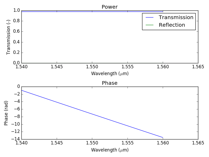
Frequency-domain response of a waveguide.
Building a circuit
A circuit consists of 3 things:
Instances of other cells,
Nets that describe how these instances are connected,
Terms (terminals) that define the interface of the circuit to the outside world.
To illustrate this, we’ll use the standard ConnectComponents.
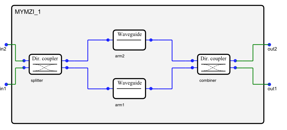
A Mach-Zehnder Interferometer.
arm1 = MyWaveguide()
arm1.CircuitModel(length=100)

arm2 = MyWaveguide()
arm2.CircuitModel(length=200)

splitter = MyDC()
splitter.CircuitModel()

combiner = MyDC()
combiner.CircuitModel()

mzi = i3.ConnectComponents(
    child_cells={
        'arm1': arm1,
        'arm2': arm2,
        'splitter': splitter,
        'combiner': combiner
    },
    links=[
        ('splitter:out1', 'arm1:in'),
        ('splitter:out2', 'arm2:in'),
        ('combiner:in1', 'arm1:out'),
        ('combiner:in2', 'arm2:out')
    ],
    external_port_names={
        "splitter:in1": "in1",
        "splitter:in2": "in2",
        "combiner:out1": "out1",
        "combiner:out2": "out2"
})
That’s it! We can now run a simulation:
mzi = MyMZI()
mzi_cm = mzi.CircuitModel()
wavelengths = np.linspace(1.54, 1.56, 1001)
S = mzi_cm.get_smatrix(wavelengths)
If we plot the results we’ll see the typical sinusoidal curve for a MZI. Increasing the delay difference will decrease the FSR.
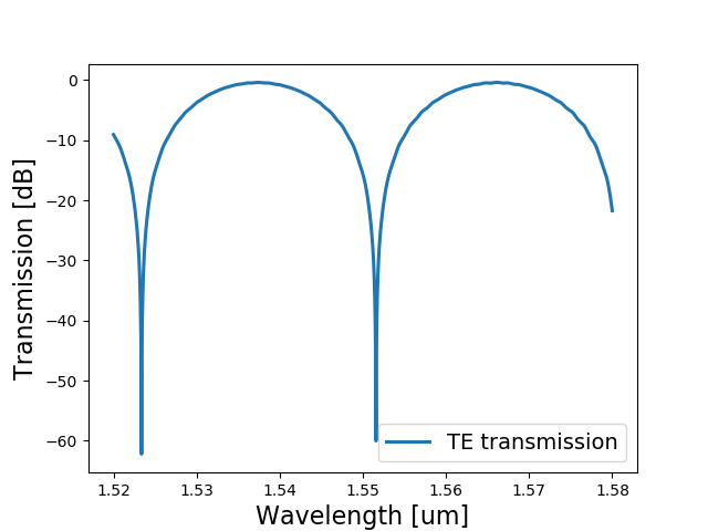
Frequency-domain response of the Mach-Zehnder Interferometer (MZI).
Download the full example here.
Note
ConnectComponents is used to simply connect devices.
See the Placement and routing page for more placement / routing functions
available in IPKISS.
Adding time-domain behavior
A compact model can include arbitrary time-dependent contributions, and state variables that introduce dynamical behavior (such as temperature, gain, energy inside a resonator). Two functions are added to the compact model to enable a time-domain model:
calculate_signals(parameters, env, output_signals, y, t, input_signals)This function has to set the
output_signalsas function of theinput_signals, state variables (y), and the time. Theinput_signalscontains the input at each port of the device, and can be accessed on each timestep (this allows to define delays). For example,input_signals['in', t - delay].calculate_dydt(parameters, env, dydt, y, t, input_signals)This function defines the ordinary differential equations through
dy/dt, so it has to setdydt.yrepresents the states of the component (they are not to be confused with ports). They are used to describe dynamic effects. For example, temperature effects, carriers (in a modulator), optical gain (in an SOA), states of a laser, etc. They can also describe the states of an IIR filter or state space model.
We update the original example and add a temperature-dependent, voltage dependent contribution to the phase of the waveguide. This includes a time delay caused by the length of the waveguide.
import ipkiss3.all as i3
import numpy as np
from scipy.constants import speed_of_light

class WGModel(i3.CompactModel):
    parameters = [
       'n_eff',
       'n_g',
       'length',
    ]

    terms = [
       i3.OpticalTerm(name='in'),
       i3.OpticalTerm(name='out'),
       i3.ElectricalTerm(name='el_in')
    ]

    states = [
       'temperature',
    ]

    def calculate_smatrix(parameters, env, S):
        # the value of length and n_eff are avalaible through the 'parameters' object.
        phase = 2 * np.pi / env.wavelength * parameters.n_eff * parameters.length
        A = 0.99 # the amplitude is hardcoded, but we could make it a property aswell
        S['in', 'out'] = S['out', 'in'] = A * np.exp(1j * phase)

    def calculate_signals(parameters, env, output_signals, y, t, input_signals):
        A = 0.99
        alpha = 0.1
        beta = 0.1
        # First-order approximation of the delay
        delay = parameters.length / speed_of_light * parameters.n_g
        phase = 2 * np.pi / env.wavelength * parameters.n_eff * parameters.length
        phase += alpha * input_signals['el_in']
        phase += beta * y['temperature']
        output_signals['out'] = A * np.exp(1j * phase) * input_signals['in', t - delay]
        output_signals['in'] = A * np.exp(1j * phase) * input_signals['out', t - delay]

    def calculate_dydt(parameters, env, dydt, y, t, input_signals):
        tau = 1.0
        dydt['temperature'] = -1 / tau * y['temperature'] + 0.1 * input_signals['in']


class MyWaveguide(i3.PCell):

    class Netlist(i3.NetlistView):
        def _generate_netlist(self, nl):
            nl += i3.OpticalTerm(name='in')
            nl += i3.OpticalTerm(name='out')
            nl += i3.ElectricalTerm(name='el_in')
            return nl

    class CircuitModel(i3.CircuitModelView):
        n_eff = i3.PositiveNumberProperty(doc="Effective index", default=2.4)
        n_g = i3.PositiveNumberProperty(doc="Effective index", default=4.3)
        length = i3.PositiveNumberProperty(doc="Waveguide length", default=100)

        def _generate_model(self):
            return WGModel(n_eff=self.n_eff,
                           n_g=self.n_g,
                           length=self.length)
To simulate the time response of this waveguide we first need to setup a testbench to specify which kind of signal to apply to the terms. You can construct a simple testbench using the ConnectComponents pcell.
def elec_signal(t):
    if t > 0.2:
       return 1.0
    return 0.0


def opt_signal(t):
    return 1.0


testbench = i3.ConnectComponents(
    child_cells={
        'el_excitation': i3.FunctionExcitation(port_domain=i3.ElectricalDomain,
                                               excitation_function=elec_signal),

        'opt_excitation': i3.FunctionExcitation(port_domain=i3.OpticalDomain,
                                               excitation_function=opt_signal),
        'wg': MyWaveguide(),
        'wg_out': i3.Probe(port_domain=i3.OpticalDomain),
    },
    links=[
        ('el_excitation:out', 'wg:el_in'),
        ('opt_excitation:out', 'wg:in'),
        ('wg:out', 'wg_out:in'),
    ]
)

from pylab import plt
tb_cm = testbench.CircuitModel()
result = tb_cm.get_time_response(t0=0, t1=1, dt=0.1, center_wavelength=1.55)

plt.plot(result.timesteps, result['opt_excitation'], 'g--')
plt.plot(result.timesteps, result['wg_out'])
plt.show()
Writing multimode models
To build a multimode model, the following changes are made:
The OpticalTerm has to define the number of modes through the n_modes parameter.
in calculate_smatrix: you can index the ports using
S['in:0', 'out:0'], … Indexing the modes is done numerically. For example, mode 0 represents the first TE mode, mode 1 represents the first TM mode, and so on.S['in' 'in']is equivalent toS['in:0', 'in:0'].
import ipkiss3.all as i3
import numpy as np

class MultiModeWGModel(i3.CompactModel):
    parameters = [
       'n_eff',
       'length'
    ]

    terms = [
       i3.OpticalTerm(name='in', n_modes=2),
       i3.OpticalTerm(name='out', n_modes=2),
    ]

    def calculate_smatrix(parameters, env, S):
        phase0 = np.exp(1j * 2 * np.pi / env.wavelength * parameters.n_eff[0] * parameters.length)
        phase1 = np.exp(1j * 2 * np.pi / env.wavelength * parameters.n_eff[1] * parameters.length)
        A = 0.99
        S['in:0', 'out:0'] = A * phase0
        S['in:1', 'out:1'] = A * phase1
        S['out:0', 'in:0'] = A * phase0
        S['out:1', 'in:1'] = A * phase1


class MyWaveguide(i3.PCell):

    class Netlist(i3.NetlistView):
        def _generate_netlist(self, nl):
            nl += i3.OpticalTerm(name='in', n_modes=2)
            nl += i3.OpticalTerm(name='out', n_modes=2)
            return nl

    class CircuitModel(i3.CircuitModelView):
        n_eff = i3.NumpyArrayProperty(doc="Effective indices for all modes")
        length = i3.PositiveNumberProperty(doc="Waveguide length", default=100)

        def _default_n_eff(self):
            return np.asarray([2.4, 2.5])

        def _generate_model(self):
            return MultiModeWGModel(n_eff=self.n_eff,
                                    length=self.length)

wavelengths = np.linspace(1.54, 1.56, 1001)
wg = MyWaveguide()
wg_cm = wg.CircuitModel()
S = wg_cm.get_smatrix(wavelengths)

from pylab import plt
plt.subplot(211)
plt.title('Power')
plt.plot(wavelengths, np.abs(S['in:0', 'out:0'])**2, label='Transmission, mode 0')
plt.plot(wavelengths, np.abs(S['in:1', 'out:1'])**2, label='Transmission, mode 1')
plt.legend()
plt.subplot(212)
plt.title('Phase')
plt.plot(wavelengths, np.unwrap(np.angle(S['in:0', 'out:0'])), label='Transmission')
plt.plot(wavelengths, np.unwrap(np.angle(S['in:1', 'out:1'])), label='Transmission')

plt.show()
Download the full example here.
Specifying default values for parameters
To avoid having to specify the values of the parameters each time you want to use a model, you can specify default values in the following way:
import ipkiss3.all as i3
import numpy as np

class WGModel(i3.CompactModel):
    """ A simple waveguide model.
    """

    parameters = [
       'n_eff',
       'length',
    ]

    # we use a default value of 2.4 for n_eff
    n_eff = 2.4

    terms = [
       i3.OpticalTerm(name='in'),
       i3.OpticalTerm(name='out'),
    ]

    def calculate_smatrix(parameters, env, S):
        phase = 2 * np.pi / env.wavelength * parameters.n_eff * parameters.length
        A = 0.99
        S['in', 'out'] = S['out', 'in'] = A * np.exp(1j * phase)

# now you only need to specify the length when using the WGModel:

class MyWaveguide(i3.PCell):
    class Netlist(i3.NetlistView):
        def _generate_netlist(self, nl):
            nl += i3.OpticalTerm(name='in')
            nl += i3.OpticalTerm(name='out')
            return nl

    class CircuitModel(i3.CircuitModelView):
        n_eff = i3.PositiveNumberProperty(doc="Effective index", default=2.4)
        length = i3.PositiveNumberProperty(doc="Waveguide length", default=100)

        def _generate_model(self):
            return WGModel(length=self.length)
Default values can come in handy when you want to declare a range of models in your PDK, each with a different set of property values. As an example, let’s see how we can define several waveguide types:
class WGTypeAModel(WGModel):
    """Use the docstring to add a short description.
    """
    n_eff = 2.39

class WGTypeBModel(WGModel):

    n_eff = 2.41
Accessing the layout from the model view
In IPKISS, you can run circuit simulations where the information of the layout is reused during the circuit simulation. More specifically, within the same IPKISS PCell, the CircuitModel view will extract information from the Layout view.
In IPKISS, waveguide models automatically extract the length from the layout. This is especially useful in templated classes that assist in creating circuits, such as i3.Circuit and/or IoFibcoup.
Note
In previous versions of IPKISS (<= 3.1.2), you had to manually set the waveguide behavior:
import ipkiss3.all as i3
i3.Waveguide.set_default_view("CapheModelFromLayout")
i3.RoundedWaveguide.set_default_view("CapheModelFromLayout")
To access layout information from within a CircuitModelView, you can use the .layout_view attribute to access the layout of your component:
    class CircuitModel(i3.CircuitModelView):
        length = i3.PositiveNumberProperty(doc="Waveguide length")
        n_eff = i3.PositiveNumberProperty(doc="Effective index", default=2.4)

        def _default_length(self):
            # The length is calculated from the layout shape (which is extracted from layout_view)
            shape = self.layout_view.shape
            return shape.length()

        def _generate_model(self):
            return WGModel(length=self.length, n_eff=self.n_eff)
You can download the full example here.
Running simulations
There are currently two simulation modes: frequency domain simulation and a transient time-domain simulation.
Running a frequency-domain simulation
If you are interested in the linear response of a device under test, you can use the get_smatrix function of a CircuitModelView. For example, if you have a PCell called MyMZI (as in the example above), you can do:
mzi = MyMZI()
mzi_cm = mzi.CircuitModel()
wavelengths = np.linspace(1.54, 1.56, 1001)
S = mzi_cm.get_smatrix(wavelengths)
This will run a simulation from 1.54 um to 1.56 um, equally spaced over 1001 steps. The resulting object is a 3D matrix that can be accessed name-based. For example, S['out1', 'in1'] is a 1D array (as a function of wavelength), that describes the transmission from port in1 to port out1.
Under the hood, get_smatrix constructs a testbench, which connects every term of the circuit to a monitor (i3.Probe).
Running a time-domain simulation
Running a time-domain simulation (transient), requires a user to set up a testbench. A testbench contains excitations and monitors, similar to how you would build a testbench in the electronic domain. Here’s a simple example of how you could embed a ‘laser’ with one electrical input (current) and one optical output:
testbench = i3.ConnectComponents(
    child_cells={
        'excitation': i3.FunctionExcitation(port_domain=i3.ElectricalDomain, excitation_function=my_func)
        'laser': laser,
        'output_signal': i3.Probe(port_domain=i3.OpticalDomain)
    },
    links=[
        ('excitation:out', 'laser:in'),
        ('laser:out', 'output_signal:in'),
    ]
)
Currently, the following two pcells are available to build a testbench:
i3.FunctionExcitation: this is used to excite a port using a given user-defined function f(t). It has one portout.i3.Probe: this is used to ‘monitor’ the time trace that enters this device. It has one portin.
Once you have defined the circuit, you can instantiate the CircuitModelView, and then run a transient simulation with the get_time_response command:
tb_cm = testbench.CircuitModel()
result = tb_cm.get_time_response(t0=0, t1=1, dt=0.1, center_wavelength=1.55)

from pylab import plt
plt.plot(result.timesteps, result['output_signal'])
plt.show()
get_time_response accepts the following arguments:
t0, t1, dt: floats, representing the start time, end time, and sampling timesteps.
center_wavelength: the center wavelength at which the signals are modulated.
integration_method: currently, can be ‘euler’ or ‘runge_kutta4’.
It returns a results object that has:
An attribute
timesteps, which contain the actual sampled timesteps.For each Excitation and Probe, the values of the signal at its port. These can be accessed by name. Each Excitation or Probe inside the top-level testbench can be accessed this way based on the instance name it was given.
You can download a full time-domain simulation example here (2 files):
circuit_sim_5_timedomain +
testbench.
Additional resources
Please check out the samples in the samples folder of your installation. They are located under the circuit_simulation subfolder
Advanced topics for building models: advanced model topics
Additional topics on using S-parameter data and building models based on them: circuit models based on S-parameter data
If you want to read more on netlists: netlist
If you want to read more on circuit hierarchy: hierarchy
If you want to read more on pcells and default views: pcell