Physical Device Simulation
An important aspect in the photonics design flow is the ability to run physical simulations of (electro-)optical devices. Typical use cases are device exploration and optimizing a component for certain specifications (for example, maximal transmission, reflection below a certain dB).
In IPKISS we start from an IPKISS Component to automatically drive a simulation in a third-party simulation tool. This has the big benefit that we don’t have to rebuild the component manually in the third party tool, saving us time and reducing translation errors. In addition, Python allows another layer of automation, which means it becomes easy to perform sweeps / optimizations of these devices.
General concept
The concept of the IPKISS device simulation flow is depicted below:
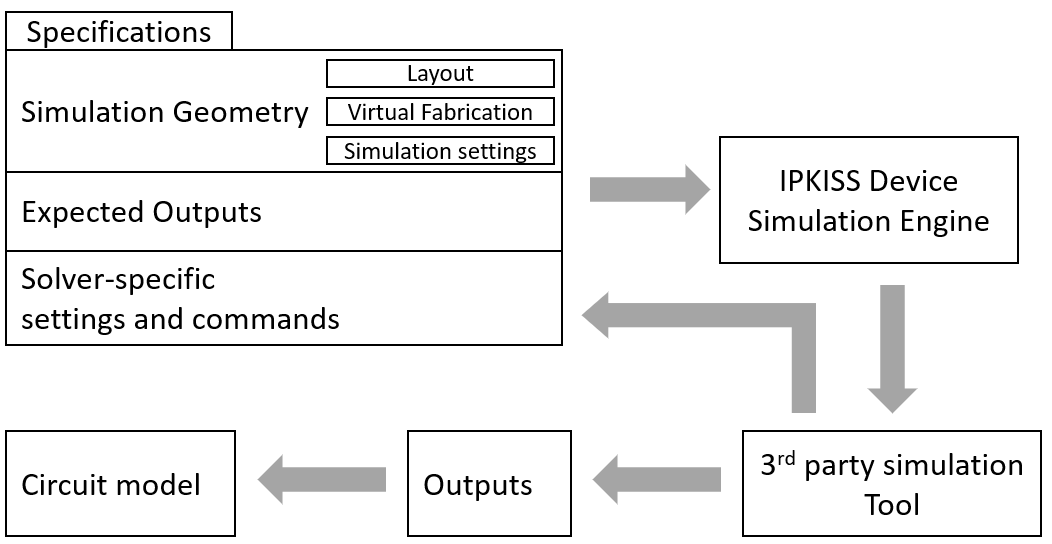
First, you define the simulation specifications, which consist of 3 parts:
The simulation geometry, defined by the layout, a virtual fabrication process, and simulation-specific settings.
The expected outputs (results) of the simulation, e.g. S Parameters.
Solver-specific settings and commands, for using the full power of the solver you want to use.
From this complete specification, IPKISS generates the input to the solver in an automated way and uses that to drive the solver. The solver generates the requested results and IPKISS ensures this output can be used further. Finally, you can use the results to generate or improve circuit models. For instance, you could fit an interpolating model to the discrete S-parameter data returned by an FDTD solver.
The basic steps
When you setup an electromagnetic simulation from within IPKISS, you go through the following steps:
Define the geometry that represents your component.
Specify the simulation job, consisting of the geometry, the expected outputs and simulation settings
Inspect the exported geometry
Retrieve the simulation results
Using a simple Multi Mode Interferometer (MMI) we’ll show how to complete each of these steps. First let us start with defining the layout of the MMI:
Define the Simulation Geometry
Create a layout
For the sake of simplicity we will import an MMI from the Picazzo library.
import si_fab.all as pdk
from picazzo3.filters.mmi.cell import MMI1x2Tapered
from picazzo3.traces.wire_wg.trace import WireWaveguideTemplate
import ipkiss3.all as i3

mmi_trace_template = WireWaveguideTemplate()
mmi_trace_template.Layout(core_width=5.0, cladding_width=10.0)

mmi_access_template = WireWaveguideTemplate()
mmi_access_template.Layout(core_width=1.0, cladding_width=10.0)

trace_template = WireWaveguideTemplate()
trace_template.Layout(core_width=0.5, cladding_width=10.0)

MMI = MMI1x2Tapered(mmi_trace_template=mmi_trace_template,
                    input_trace_template=mmi_access_template,
                    output_trace_template=mmi_access_template,
                    trace_template=trace_template,
                    )

transition_length = 20.0
mmi_length = 22.0
MMI_lo = MMI.Layout(transition_length=transition_length,
                    length=mmi_length,
                    trace_spacing=2.6)
Verifying the device geometry
Before simulating, you can verify the virtual fabrication of a device in IPKISS.
Two functions (methods of any layout view) are available for that:
visualize_2dshows a top-down view of the device geometry based on material stackscross_sectionshows a cross-section of a device along a given path
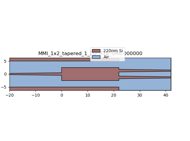
We can visualize the geometry of the MMI defined above as:
MMI_lo.visualize_2d()
xs = MMI_lo.cross_section(
  cross_section_path=i3.Shape([(10.0, -5.0), (10.0, 5.0)]),
  path_origin=-5.0
)

xs.visualize()
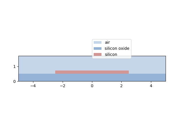
To use the cross_section() method, you need to specify the path along which to take the cross-section.
This needs to be an IPKISS Shape. You can also specify the path_origin argument in order to have a meaningful x axis.
The method returns an object which you can visualize with its visualize() method.
Both visualize_2d() and cross_section() use the default virtual fabrication process.
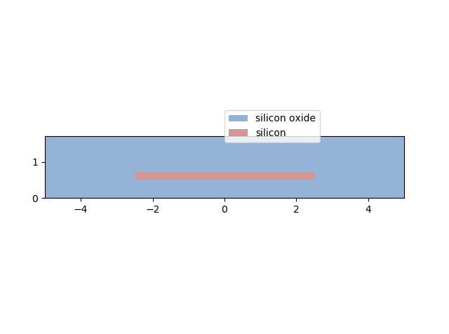
You can override this to a custom virtual fabrication process, by specifying vfabrication_process_flow in
visualize_2d() and specifying process_flow in cross_section():
MMI_lo.visualize_2d(vfabrication_process_flow=process_flow_soi_oxide)
xs = MMI_lo.cross_section(
     cross_section_path=i3.Shape([(10.0, -5.0), (10.0, 5.0)]),
     process_flow=process_flow_soi_oxide,
     path_origin=-5.0
)

xs.visualize()

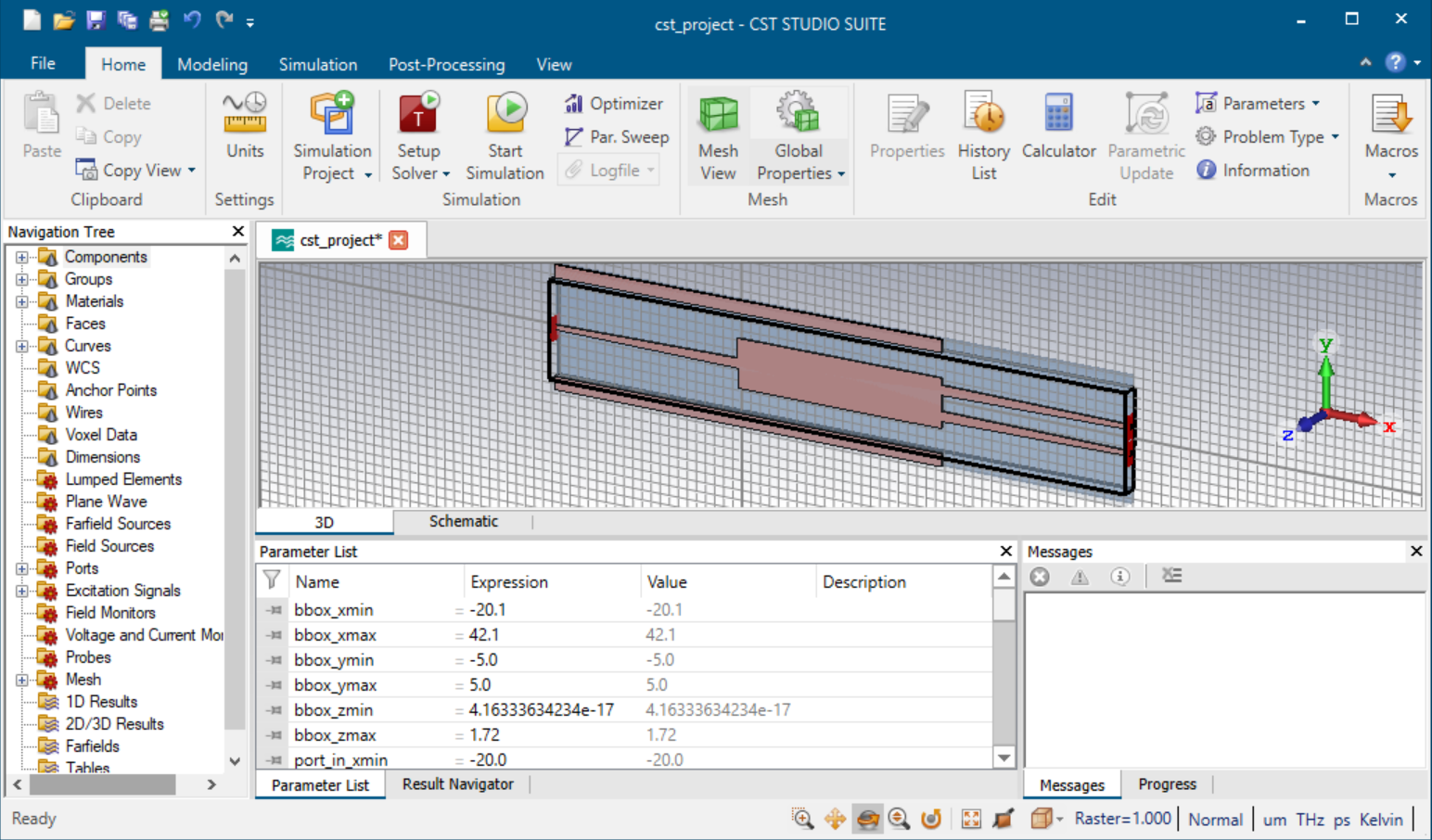
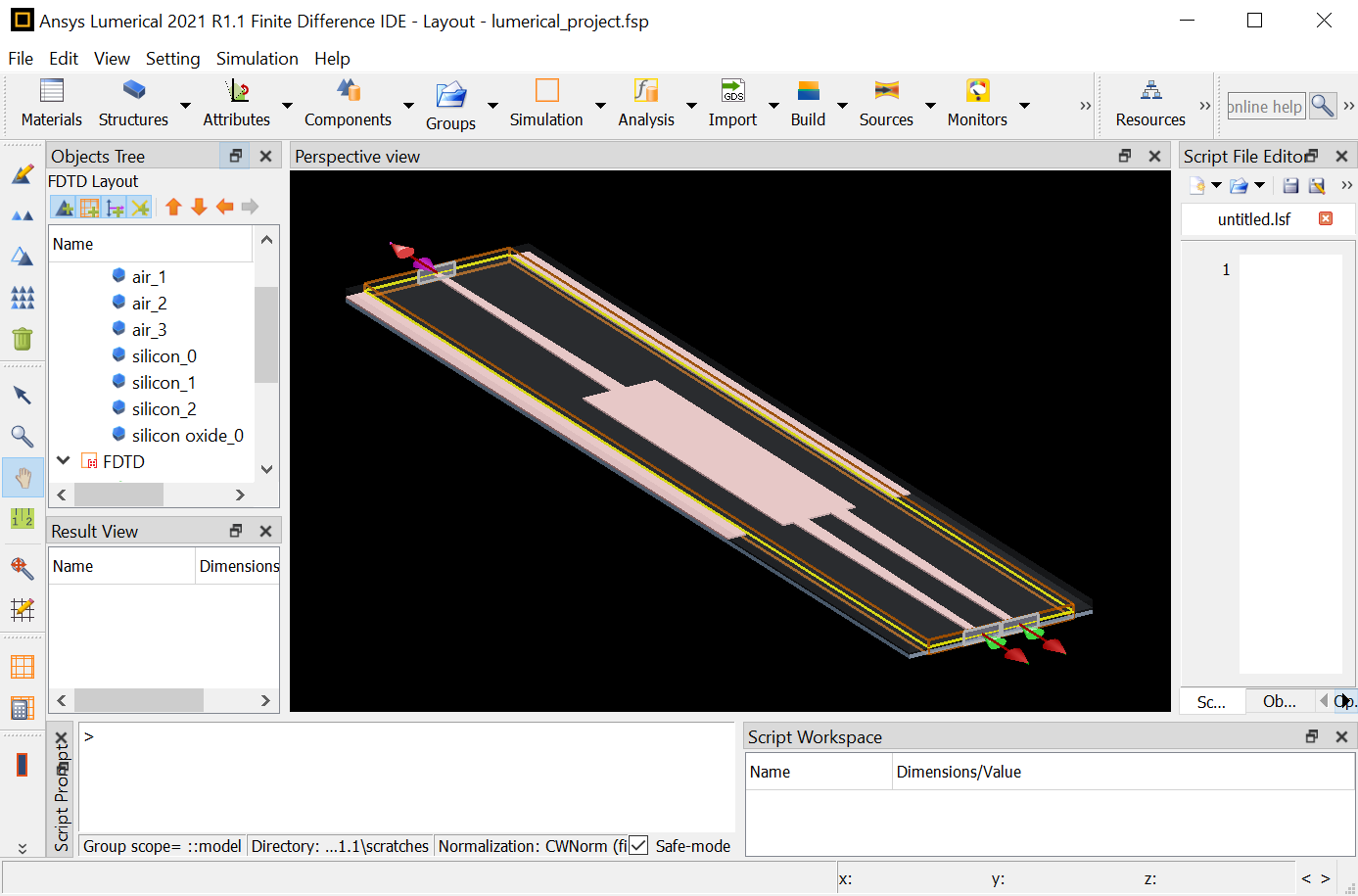
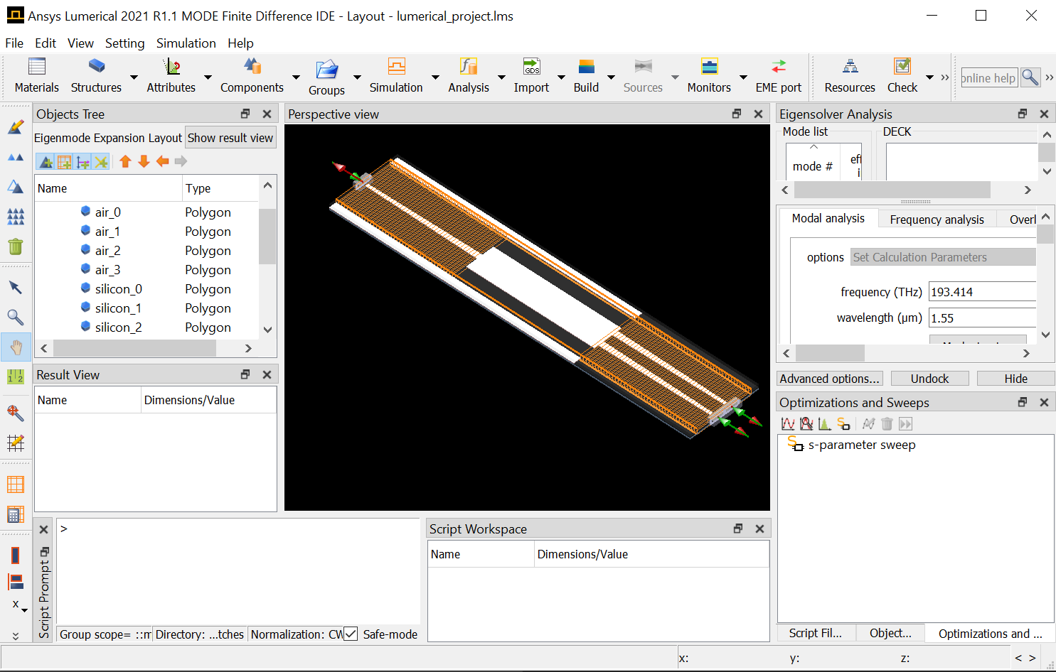
Simulation Geometry
Now that we have a layout for our component, we can use it to define the geometry of our simulation. IPKISS reuses the information it has to provide reasonable defaults, this way the initial declaration is straightforward.
sim_geom = i3.device_sim.SimulationGeometry(
    layout=MMI_lo,
)
That’s all you have to do when it comes to building the simulation geometry, IPKISS can now:
Transform the layer information in a three dimension representation.
Derive default dimensions for the simulation bounding box
Derive defaults for the position and size of the ports
Advanced geometry settings
The defaults provided by IPKISS are often sufficient for a first step when you want to get a qualitative idea of the performance of your component. To improve the accuracy or efficiency, you’ll want to tune the settings of your simulation.
Waveguide growth
It is possible to extend the waveguides:
sim_geom = i3.device_sim.SimulationGeometry(
    layout=MMI_lo,
    waveguide_growth=0.1,
)
This setting is recommended if you are planning to use run FDTD simulations where typically Perfectly Matched Layers (PMLs) are used to gradually attenuate the fields at the edge of the simulation region.
Note
This setting is not compatible with mode propagation tools (such as Ansys Lumerical MODE, when using the EME solver) and will result in inaccurate results. IPKISS will warn you when you use this combination of settings.
Process Flow
A Process Flow describes how we turn layout elements defined on layers, into a 3D representation. To create this process flow, you need information from the foundry on the relation between layers and the fabricated device. Many of the Luceda PDKs offered by foundries will contain a process flow definition. If that’s not the case or you’re using your own PDK, you can build your own. We’ve written documentation to help you doing so.
By default IPKISS will use the process flow defined in the Technology of your PDK, which is assumed to be available under i3.TECH.VFABRICATION.PROCESS_FLOW.
You can override this by providing a value for the process_flow attribute when initializing i3.device_sim.SimulationGeometry.
This allows you to experiment with variations of the material properties or the material thicknesses.
Excluding Layers
When you define the layout of a component, you sometimes use layers that you do not want export to the simulation tool.
There might be various reasons for this, these layers might be logical layers like a device recognition
layer, or you might want to exclude metal layers from your simulation. You can do this with the excluded_layers attribute.
The MMI example only contains two layers, so this concept will be demonstrated using the PhaseModulator included in Picazzo3.
import si_fab.all as pdk
from ipkiss.technology import get_technology
TECH = get_technology()
from picazzo3.modulators.phase import PhaseModulator
import ipkiss3.all as i3

pmod = PhaseModulator()
pmod_lay = pmod.Layout(length=40.)

# we declare here that we exclude all the layers that don't belong to the
# waveguide, though in a real simulation, you'll most likely do want include those.
sim_geom = i3.device_sim.SimulationGeometry(
  layout=pmod_lay,
  excluded_layers=[
      i3.TECH.PPLAYER.P.LINE,
      i3.TECH.PPLAYER.N.LINE,
      i3.TECH.PPLAYER.PPLUS.LINE,
      i3.TECH.PPLAYER.NPLUS.LINE,
      i3.TECH.PPLAYER.M1,
      i3.TECH.PPLAYER.SIL.LINE,
      i3.TECH.PPLAYER.CONTACT.PILLAR,
  ]
)
In the case of our PhaseModulator example, you’ll probably want to only list the layers you’re interested in. That’s something you can do as well:
import si_fab.all as pdk
from ipkiss.technology import get_technology
TECH = get_technology()
from picazzo3.modulators.phase import PhaseModulator
import ipkiss3.all as i3

pmod = PhaseModulator()
pmod_lay = pmod.Layout(length=40.)

sim_geom = i3.device_sim.SimulationGeometry(
  layout=pmod_lay,
  layers=[
      i3.TECH.PPLAYER.WG.CORE,
      i3.TECH.PPLAYER.WG.CLADDING,
      i3.TECH.PPLAYER.RWG.CORE,
      i3.TECH.PPLAYER.RWG.CLADDING,
  ]
)
Note
Using the layers attribute, will override the excluded_layers setting.
Bounding Box
When you don’t specify the bounding box manually, a default is calculated. This is done in such a way that all ports and elements fit within the bounding box. You can also partially modify this bounding box. This means that you only need to set those values you wish to set, otherwise the default value is kept. The example below illustrates this using the MMI defined above:
sz_info = MMI_lo.size_info()
# sz_info: west: -20.0 - east: 42.0 - south: -6.3 - north: 6.3

sim_geom = i3.device_sim.SimulationGeometry(
  layout=MMI_lo,
  bounding_box=[
    [sz_info.west - 1.0, sz_info.east + 1.0],  # x-span of the bounding box
    [-5.0, 5.0], # y-span of the bounding box, here we use the default calculated by IPKISS
    None # z-span of the bbox, here we use the default calculated by IPKISS
  ]
)
Choose a simulation tool
With just a geometry we can’t do much, to put it to use we have to pass it to a tool-specific simulator. At the moment IPKISS supports three tools, and which one to use depends on your application. Even though their API is pretty similar, the tutorial is split into parts for clarity and conciseness. Follow one of these links to continue:
|
|
|