WaveguideBundle
- class picazzo3.wg.bundle.cell.WaveguideBundle
Bundle of waveguides, routed together
- Parameters:
- traces: List with type restriction, allowed types: <class ‘ipkiss3.pcell.cell.pcell.PCell’>
the traces in this bundle
- name: String that contains only ISO/IEC 8859-1 (extended ASCII py3) or pure ASCII (py2) characters
The unique name of the pcell
Views
- class Layout
- Parameters:
- area_layer_on: ( bool, bool_ or int )
When True, the entire bundle area will be covered by all the cover layers.
- trace_transformations: list and List with type restriction, allowed types: <class ‘ipkiss.geometry.transform.Transform’>
transformations to be applied to each of the traces
- cover_layers: List with type restriction, allowed types: <class ‘ipkiss.primitives.layer.Layer’>
layers that can be used to generate additional coverage of the trace (e.g. manhattan corners)
- view_name: String that contains only alphanumeric characters from the ASCII set or contains _$. ASCII set is extended on PY3.
The name of the view
Examples
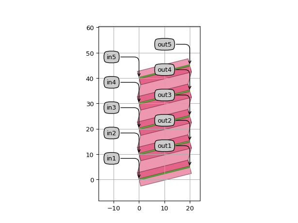
import si_fab.all as pdk  # noqa: F401
import ipkiss3.all as i3
from picazzo3.wg.bundle import WaveguideBundle
from picazzo3.traces.wire_wg.trace import WireWaveguideTemplate

wg_t = WireWaveguideTemplate()
wg_t.Layout(core_width=0.550, cladding_width=i3.TECH.WG.CLADDING_WIDTH, core_process=i3.TECH.PROCESS.WG)
trace = wg_t()
trace.Layout(shape=[(0.0, 0.0), (20.0, 5.0)])
trace_tfs = [i3.Translation(translation=(0.0, 10.0 * i)) for i in range(5)]
C = WaveguideBundle(traces=[trace] * 5)
lay = C.Layout(trace_transformations=trace_tfs)
lay.visualize(annotate=True)