W1Waveguide
- class picazzo3.phc.w1.cell.W1Waveguide
A Uniform Photonic Crystal W1 waveguide consisting of 12-sided holes. You can specify the diameter of the lattice and the diameter of the defect holes in the core of the waveguide.
It is also possible to override the parameters of DodecPhCLayout, which allows you to customize the PCell in more detail.
- Parameters:
- name: String that contains only ISO/IEC 8859-1 (extended ASCII py3) or pure ASCII (py2) characters
The unique name of the pcell
Views
- class Layout
- Parameters:
- n_o_periods: int and number > 0
Number of lattice periods in the propagation direction.
- n_o_cladding_layers: int and number > 0
Number of cladding layers north and south.
- defect_diameter: float and Real, number and number >= 0
Diameter of the defect holes. If zero, no holes are drawn.
- diameter: float and number > 0
diameter of the photonic crystal lattice holes
- purpose: PatternPurpose
Purpose of the layer on which the holes should be drawn.
- process_wg: ProcessLayer
Process of the layer on which the holes should be drawn.
- hole_sizes: dict
dictionary of the hole sizes of the Photonic Crystal. The value should be of the form {‘x’: 0.25, ‘y’: 0.26}. The keys of the dictionary should be characters and each character can be used to identify the unit cell in the map. If the property ‘cells’ is set manually, hole_sizes’ will be ignored.
- pitch: float and Real, number and number >= 0
Lattice constant for a uniform triangular lattice. This property will be ignored if ‘lattice_pitches’ or ‘pitches’ are set manually
- lattice_pitches: Coord2 and number >= 0
Lattice constants along the horizontal and the oblique direction. Choose identical values for a regular grid. If ‘pitches’ is manually set, this property will be ignored. If this property is set, the property ‘pitch’ will be ignored.
- ports_coordinates:
list of tuple with (coordinate (in pitches), angle, waveguide_template, [name])
- zero_line_y: float
line in the map which corresponds to the coordinate y=0. This can be a fractional number, and the unit is relative to pitches.y .
- purpose_hfw: PatternPurpose
drawing purpose for underetching
- process_hfw: ProcessLayer
process for underetching
- map: str and String that contains only ISO/IEC 8859-1 (extended ASCII py3) or pure ASCII (py2) characters
Map of the photonic crystal. This property accepts a multi-line string. Every character in the string represents a unit cell of the photonic crystal, which can be found in the property cells
- cells:
dictionary of Unit Cells for a Photonic Crystal. The value should be of the form {‘x’: cell1, ‘y’: cell2}. The keys of the dictionary should be characters and each character can be used to identify the unit cell in the map. The default value of this property is automatically calculated from the dictionary ‘hole_sizes’. Only assign to this property if you want to override this value. If you do this, the property ‘hole_sizes’ will be ignored.
- pitches:
Cartesian (X, Y) pitches of the lattice. If this is specified, the properties ‘lattice_pitches’ and ‘pitch’ will be ignored
- view_name: String that contains only alphanumeric characters from the ASCII set or contains _$. ASCII set is extended on PY3.
The name of the view
Examples
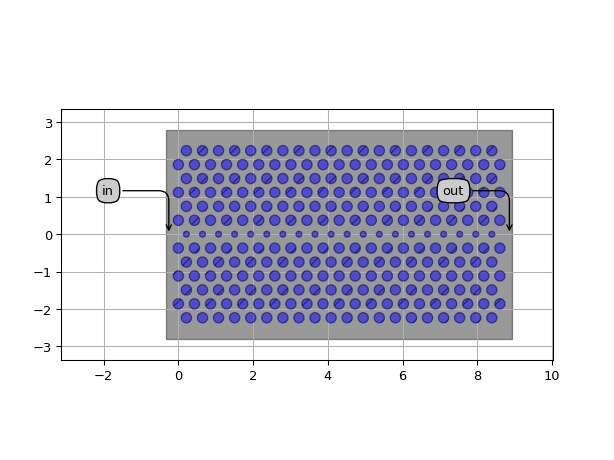
"""A W1 waveguide with a missing row of holes"""
import si_fab.all as pdk  # noqa: F401
from picazzo3.phc.w1 import W1Waveguide

cell = W1Waveguide(name="my_w1")
layout = cell.Layout(
    pitch=0.43,  # lattice period of the triangular lattice
    diameter=0.28,  # hole diameter of the lattice
    n_o_cladding_layers=5,  # number of rows on each side of the defect
    n_o_periods=20,  # length of the lattice
)

layout.visualize(annotate=True)
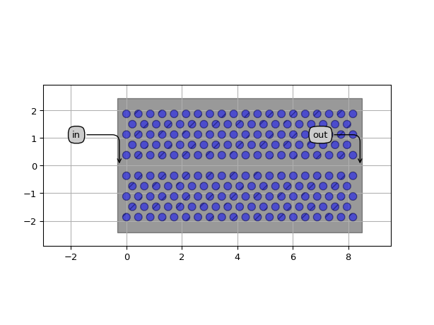
"""A W1 waveguide with a center row of holes of different size"""
import si_fab.all as pdk  # noqa: F401
from picazzo3.phc.w1 import W1Waveguide

cell = W1Waveguide(name="my_w1_with_defect")
layout = cell.Layout(
    pitch=0.43,  # lattice period of the triangular lattice
    diameter=0.28,  # hole diameter of the lattice
    defect_diameter=0.16,  # defect hole diameter
    n_o_cladding_layers=6,  # number of rows on each side of the defect
    n_o_periods=21,  # length of the lattice
)

layout.visualize(annotate=True)