OctPhCLayout
- class picazzo3.phc.generic.cell.OctPhCLayout
Generic Layouting cell for Photonic Crystals with octagon holes on a Rectangular lattice. The Layout of the cell is made up of a map, which is a multiline string representing the unit cells on a regular rectangular lattice. The letters in the ‘map’ correspond to the diameters of the holes in the dictionary ‘hole_sizes’.
- Parameters:
- name: String that contains only ISO/IEC 8859-1 (extended ASCII py3) or pure ASCII (py2) characters
The unique name of the pcell
See also
Views
- class Layout
- Parameters:
- process_wg: ProcessLayer
Process of the layer on which the holes should be drawn.
- hole_sizes: dict
dictionary of the hole sizes of the Photonic Crystal. The value should be of the form {‘x’: 0.25, ‘y’: 0.26}. The keys of the dictionary should be characters and each character can be used to identify the unit cell in the map. If the property ‘cells’ is set manually, hole_sizes’ will be ignored.
- purpose: PatternPurpose
Purpose of the layer on which the holes should be drawn.
- pitch: float and Real, number and number >= 0
Lattice constant for a uniform square lattice. This property will be ignored if the property ‘pitches’ is set manually
- ports_coordinates:
list of tuple with (coordinate (in pitches), angle, waveguide_template, [name])
- zero_line_y: float
line in the map which corresponds to the coordinate y=0. This can be a fractional number, and the unit is relative to pitches.y .
- purpose_hfw: PatternPurpose
drawing purpose for underetching
- process_hfw: ProcessLayer
process for underetching
- map: str and String that contains only ISO/IEC 8859-1 (extended ASCII py3) or pure ASCII (py2) characters
Map of the photonic crystal. This property accepts a multi-line string. Every character in the string represents a unit cell of the photonic crystal, which can be found in the property cells
- cells:
dictionary of Unit Cells for a Photonic Crystal. The value should be of the form {‘x’: cell1, ‘y’: cell2}. The keys of the dictionary should be characters and each character can be used to identify the unit cell in the map. The default value of this property is automatically calculated from the dictionary ‘hole_sizes’. Only assign to this property if you want to override this value. If you do this, the property ‘hole_sizes’ will be ignored.
- pitches: Coord2 and number >= 0
X and Y pitch of the photonic crystal
- view_name: String that contains only alphanumeric characters from the ASCII set or contains _$. ASCII set is extended on PY3.
The name of the view
Examples
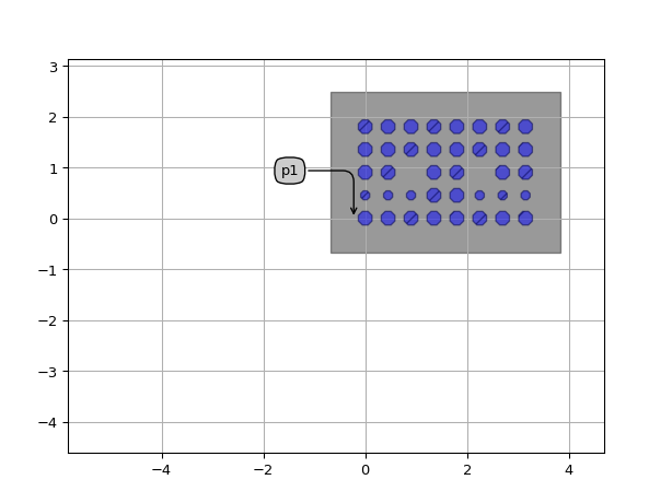
import si_fab.all as pdk  # noqa: F401
from ipkiss3 import all as i3

TECH = i3.TECH
from picazzo3.phc.generic import OctPhCLayout

my_phc_map = ["AAAAAAAA", "AAAAAAAA", "AA AA AA", "BBBAABBB", "AAAAAAAA"]
cell = OctPhCLayout(name="my_oct_phc_layout1")
layout = cell.Layout(
    pitch=0.45,
    hole_sizes={"A": 0.290, "B": 0.190},  # two sizes
    map="\n".join(my_phc_map),
    zero_line_y=5,  # count lines from the top
    ports_coordinates=[
        ((-0.5, 0), 180, TECH.PCELLS.WG.DEFAULT),
        ((10.5, 0), 0, TECH.PCELLS.WG.DEFAULT),
    ],  # coordinates expressed in lattice pitches
)

layout.visualize(annotate=True)