ContactHole
- class picazzo3.electrical.contact.cell.ContactHole
Regular via to connect M1 (
top_layer) to the silicide layer (bottom_layer) using a contact layer (via_layer)- Parameters:
- name: String that contains only ISO/IEC 8859-1 (extended ASCII py3) or pure ASCII (py2) characters
The unique name of the pcell
Views
- class Layout
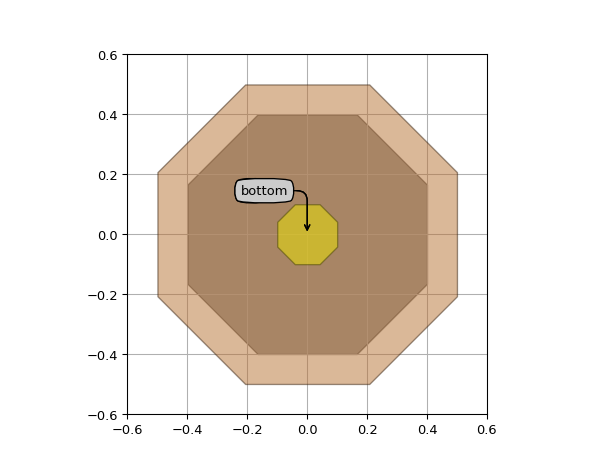
A standard electrical via connect M1 (
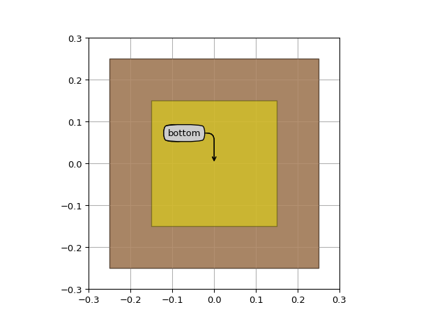
top_layer) to the silicide layer (bottom_layer) using a contact layer (via_layer).The shape of each layer in the via is a regular polygon with a
n_o_sidessides. and each layer element (top,bottomandvia) is defined through the following properties:top_process
top_purpose
top_width
analogous properties are defined for the other layers.
All those properties can be overridden, but they are defaulting to the values found in TECH.VIAS.CONTACT_HOLE
- Parameters:
- via_width: float and number > 0
Width of the
vialayer (2 * inner radius of the polygon)- via_purpose: PatternPurpose
Purpose of the
vialayer.- via_process: ProcessLayer
Process of the
vialayer.- bottom_width: float and number > 0
Width of the
bottomlayer (2 * inner radius of the polygon)- bottom_purpose: PatternPurpose
Purpose of the
bottomlayer.- bottom_process: ProcessLayer
Process of the
bottomlayer.- top_width: float and number > 0
Width of the
toplayer (2 * inner radius of the polygon)- top_purpose: PatternPurpose
Purpose of the
toplayer.- top_process: ProcessLayer
Process of the
toplayer.- n_o_sides: int and number > 0
Number of sides of the polygon used for the contact hole
- view_name: String that contains only alphanumeric characters from the ASCII set or contains _$. ASCII set is extended on PY3.
The name of the view
- Other Parameters:
- via_shape: locked
- via_layer: locked
- layers: locked
- shapes: locked
- bottom_shape: locked
- bottom_layer: locked
- top_shape: locked
- top_layer: locked
Examples
# Using the default contact hole.
import si_fab.all as pdk  # noqa: F401
from picazzo3.electrical.contact import ContactHole

cell = ContactHole()
layout = cell.Layout()
layout.visualize(annotate=True)
import si_fab.all as pdk  # noqa: F401
from picazzo3.electrical.contact import ContactHole

cell = ContactHole()
layout = cell.Layout(n_o_sides=8, top_width=1.0, bottom_width=0.8, via_width=0.2)
layout.visualize(annotate=True)