tyndall_packaging.all.UniformPackagingArray
- class tyndall_packaging.all.UniformPackagingArray
The packaging array with the same grating components used for each grating. The packaging array automatically checks for a large number of packaging design rules.
- Parameters:
- grating: PCell
grating used in this design.
- out_name: str and String that contains only ISO/IEC 8859-1 (extended ASCII py3) or pure ASCII (py2) characters
name of the out port in the grating classes
- n_o_south_bondpads: int and number >= 0 and [0,11[
Number of south_bondpads
- n_o_north_bondpads: int and number >= 0 and [0,11[
Number of north_bondpads
- n_o_user_west_gratings: int and number >= 0
Number of user gratings in the west - without the shunt gratings.
- n_o_user_east_gratings: int and number >= 0
Number of user gratings in the east - without the shunt gratings.
- bondpad: PCell, *None allowed*
bondpad used
- name: String that contains only ISO/IEC 8859-1 (extended ASCII py3) or pure ASCII (py2) characters
The unique name of the pcell
- Other Parameters:
- west_gratings: locked
- east_gratings: locked
- shunt_grating_east: locked
- shunt_grating_west: locked
from si_fab import technology
from tyndall_packaging.all import UniformPackagingArray

lo = UniformPackagingArray().Layout()
lo.visualize(annotate=True)
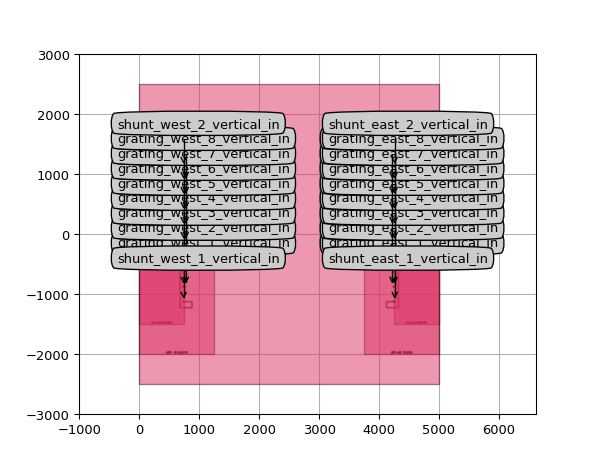
Ports
Name |
Type |
Position |
Angle |
Waveguide Template |
Inclination |
|---|---|---|---|---|---|
grating_east_1_out |
Optical |
(4225.0, -875.0) |
180.0 |
SiWireWaveguideTemplate |
0.0 |
grating_east_1_vertical_in |
Optical |
(4262.0, -875.0) |
0.0 |
90.0 |
|
grating_east_2_out |
Optical |
(4225.0, -625.0) |
180.0 |
SiWireWaveguideTemplate |
0.0 |
grating_east_2_vertical_in |
Optical |
(4262.0, -625.0) |
0.0 |
90.0 |
|
grating_east_3_out |
Optical |
(4225.0, -375.0) |
180.0 |
SiWireWaveguideTemplate |
0.0 |
grating_east_3_vertical_in |
Optical |
(4262.0, -375.0) |
0.0 |
90.0 |
|
grating_east_4_out |
Optical |
(4225.0, -125.0) |
180.0 |
SiWireWaveguideTemplate |
0.0 |
grating_east_4_vertical_in |
Optical |
(4262.0, -125.0) |
0.0 |
90.0 |
|
grating_east_5_out |
Optical |
(4225.0, 125.0) |
180.0 |
SiWireWaveguideTemplate |
0.0 |
grating_east_5_vertical_in |
Optical |
(4262.0, 125.0) |
0.0 |
90.0 |
|
grating_east_6_out |
Optical |
(4225.0, 375.0) |
180.0 |
SiWireWaveguideTemplate |
0.0 |
grating_east_6_vertical_in |
Optical |
(4262.0, 375.0) |
0.0 |
90.0 |
|
grating_east_7_out |
Optical |
(4225.0, 625.0) |
180.0 |
SiWireWaveguideTemplate |
0.0 |
grating_east_7_vertical_in |
Optical |
(4262.0, 625.0) |
0.0 |
90.0 |
|
grating_east_8_out |
Optical |
(4225.0, 875.0) |
180.0 |
SiWireWaveguideTemplate |
0.0 |
grating_east_8_vertical_in |
Optical |
(4262.0, 875.0) |
0.0 |
90.0 |
|
grating_west_1_out |
Optical |
(775.0, -875.0) |
0.0 |
SiWireWaveguideTemplate |
0.0 |
grating_west_1_vertical_in |
Optical |
(738.0, -875.0) |
180.0 |
90.0 |
|
grating_west_2_out |
Optical |
(775.0, -625.0) |
0.0 |
SiWireWaveguideTemplate |
0.0 |
grating_west_2_vertical_in |
Optical |
(738.0, -625.0) |
180.0 |
90.0 |
|
grating_west_3_out |
Optical |
(775.0, -375.0) |
0.0 |
SiWireWaveguideTemplate |
0.0 |
grating_west_3_vertical_in |
Optical |
(738.0, -375.0) |
180.0 |
90.0 |
|
grating_west_4_out |
Optical |
(775.0, -125.0) |
0.0 |
SiWireWaveguideTemplate |
0.0 |
grating_west_4_vertical_in |
Optical |
(738.0, -125.0) |
180.0 |
90.0 |
|
grating_west_5_out |
Optical |
(775.0, 125.0) |
0.0 |
SiWireWaveguideTemplate |
0.0 |
grating_west_5_vertical_in |
Optical |
(738.0, 125.0) |
180.0 |
90.0 |
|
grating_west_6_out |
Optical |
(775.0, 375.0) |
0.0 |
SiWireWaveguideTemplate |
0.0 |
grating_west_6_vertical_in |
Optical |
(738.0, 375.0) |
180.0 |
90.0 |
|
grating_west_7_out |
Optical |
(775.0, 625.0) |
0.0 |
SiWireWaveguideTemplate |
0.0 |
grating_west_7_vertical_in |
Optical |
(738.0, 625.0) |
180.0 |
90.0 |
|
grating_west_8_out |
Optical |
(775.0, 875.0) |
0.0 |
SiWireWaveguideTemplate |
0.0 |
grating_west_8_vertical_in |
Optical |
(738.0, 875.0) |
180.0 |
90.0 |
|
shunt_east_1_vertical_in |
Optical |
(4262.0, -1125.0) |
0.0 |
90.0 |
|
shunt_east_2_vertical_in |
Optical |
(4262.0, 1125.0) |
0.0 |
90.0 |
|
shunt_west_1_vertical_in |
Optical |
(738.0, -1125.0) |
180.0 |
90.0 |
|
shunt_west_2_vertical_in |
Optical |
(738.0, 1125.0) |
180.0 |
90.0 |
Circuit
Parameters
layout_view: ( _LayoutView ), None allowed
netlist_view: ( NetlistView ), None allowed
- view_name: String that contains only alphanumeric characters from the ASCII set or contains _$. ASCII set is extended on PY3.
The name of the view
Other Parameters
- solver: str and String that contains only ISO/IEC 8859-1 (extended ASCII py3) or pure ASCII (py2) characters, locked
circuit solver to use
Layout
Parameters
- doc_layer: __Layer__
Layer used for doc in the technology
- grating_offset_west: float
Grating offset on the west
- grating_offset_east: float
Grating offset on the east
- draw_die: ( bool, bool_ or int )
Draw the die
- draw_epoxy_exclusion: ( bool, bool_ or int )
Draw epoxy exclusion zones.
- draw_exclusion: ( bool, bool_ or int )
draw exclusions zone or not.
- distance_shunt: float and number > 0
Distance the shunt waveguide is doing before turning.
- bondpad_offset_south: float
x offset of the South bondpad array
- bondpad_offset_north: float
x offset of the North bondpad array
- bondpad_to_edge_south: float and number > 0 and [50.0,500.0]
Distance between the edge of the die and the south edge of the bondpad
- bondpad_to_edge_north: float and number > 0 and [50.0,500.0]
Distance between the edge of the die and the north edge of the bondpad
- bondpad_rotation: float
rotation to be applied to the bondpad before placement
bondpad_transformation: GenericNoDistortTransform
- bondpad_pitch_south: float and number > 0
Pitch between the bondpads at the south.
- bondpad_pitch_north: float and number > 0
Pitch between the bondpads at the north.
- die_height: float and number > 0
Width of the die.
- die_width: float and number > 0
Width of the die.
- grating_pitch_array_west: float and number > 0 and List with value restriction, allowed values: [127.0, 250.0]
pitch on the west.
- grating_pitch_array_east: float and number > 0 and List with value restriction, allowed values: [127.0, 250.0]
pitch on the east.
- view_name: String that contains only alphanumeric characters from the ASCII set or contains _$. ASCII set is extended on PY3.
The name of the view
Other Parameters
- min_bondpad_size: Coord2 and number >= 0, locked
Minimum size of a bondpad to override the TECH settings if allowed by a fab
- epoxy_exclusion: float and number > 0, locked
Buffer needed for epoxy overflow
- chip_edge_exclusion: float and number > 0, locked
Buffer needed at the chip edge
- die_size: tuple2, locked
Size of the die used.