Technology
Every IPKISS script starts with the import of a TECHNOLOGY file. The goal of the technology file is to describe
general settings that are stable across several designs that use the same fab.
These technology settings are managed in a tree structure, rooted in an object created by IPKISS in the module
ipkiss.technology. Each leaf of this tree we call a technology key or tech key.
Although you are free to add whatever you want to a TECHNOLOGY file the following aspects of your design process are usually described by it.
Metrics: Contains the general settings for the grid on which shapes are discretized.
Process settings: Contains all the available process layers, drawing pattern purposes, and combinations thereof: ProcessPurposeLayers
GDSII settings: Contains GDSII import and export settings.
Display settings: Contains settings that are used in visualization routines of IPKISS.
Design rules: Contains default design values for different process layers, which are used throughout IPKISS such as, minimum width, default width, default bend radius.
Materials: Materials and materials stacks
Virtual fabrication settings: Contains the description of the virtual fabrication processes that can transform a GDSII mask in a virtually fabricated structure.
Traces: Contains the description of the default waveguides that are used.
Grating Couplers: Contains the description of the default grating couplers that are used.
Required technology keys: IPKISS and PICAZZO require a number of technology settings (‘keys’) to be defined in order to work.
In this guide we will illustrate these concepts so that you can build you own technology file.
Note
This guide assumes knowledge of semiconductor process technology and terminology.
General structure of a TECH-tree
A technology in IPKISS is built as a TREE of objects of TechnologyTree
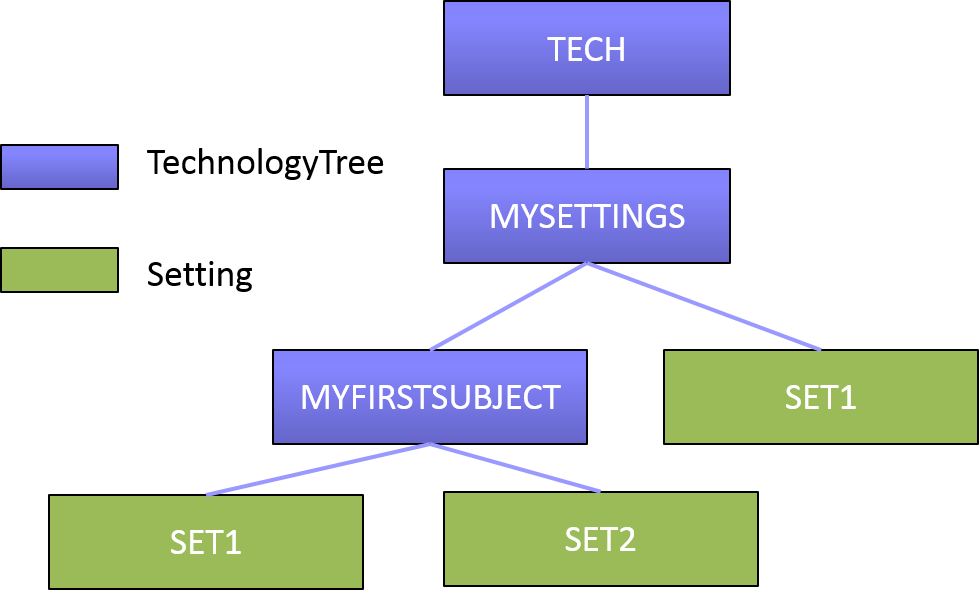
TechnologyTree
As depicted in the figure above each purple box is object of the TechnologyTree that can contain settings of any kind (depicted in green).
Creating your own TECH amounts to building up such a tree and to place the relevant settings in the leaves.
The code excerpt below illustrates this:
from ipkiss.technology import get_technology
from ipkiss.technology.technology import TechnologyTree

TECH = get_technology()
TECH.MYSETTINGS = TechnologyTree()
TECH.MYSETTINGS.SET1 = 10.0
TECH.MYSETTINGS.MYFIRSTSUBJECT = TechnologyTree()
TECH.MYSETTINGS.MYFIRSTSUBJECT.SET1 = "Hello"
TECH.MYSETTINGS.MYFIRSTSUBJECT.SET2 = 300.0


print TECH.MYSETTINGS.MYFIRSTSUBJECT.SET1
Tech settings can be any python object. In a lot of cases, you will want to store Ipkiss objects in the tech tree, e.g. default waveguides. For that purpose,
you will import a module, defining some Ipkiss class, which in its turn uses default values from the tech tree, creating a circular dependency.
These circular dependencies can be managed by using a DelayedInitTechnologyTree.
from ipkiss.technology import get_technology
from ipkiss.technology.technology import DelayedInitTechnologyTree

TECH = get_technology()

class MySettingsTree(DelayedInitTechnologyTree):
    def initialize(self):
        from mymodule import MyClass
        self.MYOBJ = MyClass()
        # now the technology tree can be fully imported at the start
        # of the main script, even if mymodule uses TECH settings

TECH.MYSETTINGS = MySettingsTree()
The initialize routine will only be called when TECH.MYSETTINGS.MYOBJ will be called. This mechanism can avoid many cases of circular dependencies.
Required technology tree
IPKISS relies on the definition of a range of technology keys for its proper functioning and tailoring to a specific technology. See the section on Required Technology Keys: IPKISS for a detailed list of required tech keys.
The required tree hierarchy is as follows. PDK developers can add their own subtrees, but the shown tree is
the minimum required for IPKISS to work.
TECH
 ├── ADMIN
 ├── METRICS
 ├── PROCESS
 ├── PURPOSE
 ├── PPLAYER
 ├── DISPLAY
 ├── GDSII
 ├── OPENACCESS
 ├── VFABRICATION
 ├── MATERIALS
 ├── MATERIAL_STACKS
 ├── PCELLS
 ├── BLOCKS
 ├── PORT
 ├── TRACE
 ├── WG_DEFAULTS
 ├── WG
 ├── VIAS
 ├── METAL
Write your own TECH: Recommended file structure
You could in theory build up you entire tree in a single Python file. However we recommend that you use the file structure that is used in the silicon photonics technology. You could for instance just start
by copying it completely and make changes gradually.
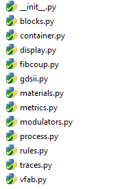
File Structure
This file structure is built up in such a way that the entire technology is imported upon the statement
import si_fab.all as pdk
In analogy, if you want to create your own technology, you can create a folder and name it after your own technology (e.g. my_custom_tech).
from technologies import my_custom_tech
will load this my_custom_tech.
As python automatically executes the __init__.py file in every module (__init__.py is needed for any python module to be discovered). All statements required to fill the technology tree
need to be written in this __init__.py file. Of course references can be made to other files to compartmentalize different aspect of the technology tree which is done in the __init__.py of the silicon
photonics.
Let’s take a look at the __init__.py file from the silicon_photonics.
# flake8: noqa

# INIT file
# Sets the technology name and loads all modules
# Be careful when changing the order of importing modules, since there may be interdependencies and risk for circular imports
# through ipkiss and/or picazzo

from ipkiss.technology import TECHNOLOGY as TECH  # Import the base technology from IPKISS.

__all__ = ["TECH"]

TECH.name = "SILICON_PHOTONICS"  # Give a name to the technology. (Required)

# Import all the other files. Each of those imports will expand the TECH tree.

from ..base_ipkiss.admin import *  # PCell name generators (Required)
from ..base_ipkiss.mask import *  # Basic mask definitions (Required)
from .metrics import *  # Drawing grid and user unit, angle discretizaion (Required)
from .process import *  # Process layers and drawing purposes (Required)
from .rules import *  # Rules for each layer (Required)
from .display import *  # Visualization settings (Required)
from .blocks import *  # Settings for blocks and adapters (Required for IOFibCoup in Picazzo)
from .container import *  # Settings for containers (Required for containers in Picazzo)
from ..base_ipkiss.pcells import *  # Basic default PCells lib (not Required)
from .traces import *  # Basic trace settings and default waveguide template (Required for Picazzo)
from .ports import *  # Basic settings for ports
from ..base_ipkiss.transitions import *  # Auto-TraceTransition database (Required for autotransitions)
from .gdsii import *  # GDSII import/export settings (Required)
from .materials import *  # Materials and material stacks (example for silicon photonics) (Required for virtual fabrication)
from .vfab import *  # Virtual fabrication flow and settings (Required for virtual fabrication)
from .fibcoup import *  # Fiber coupler settings and default coupler (Required IOFibcoup)
from .modulators import *  # Modulator settings (Required for Modulators)
from .models import *  # Import models for the awgs (Required for AWGs in spectral toolbox)
Different aspects of the TECH file are now managed by different sub-modules that are imported sequentially. We will elaborate over some of those.
Name of the technology
The first required step is to import the base TECH object from ipkiss.techonolgy and give it a name.
from ipkiss.technology import TECHNOLOGY as TECH  # Import the base technology from IPKISS.

__all__ = ["TECH"]

TECH.name = "SILICON_PHOTONICS"  # Give a name to the technology. (Required)

# Import all the other files. Each of those imports will expand the TECH tree.

from ..base_ipkiss.admin import *  # PCell name generators (Required)
from ..base_ipkiss.mask import *  # Basic mask definitions (Required)
Also the PCell name generators and basic mask definition need to be imported. It is unlikely you will need to modify those unless you want to do truly specialized things.
Metrics
Metrics are setting related to standard distance units and discretization settings. Changes here are rare, so you can perfectly copy the existing file from the silicon_photonics tech.
################
# Basic Metrics
################

from ipkiss.technology import get_technology
from ipkiss.technology.technology import TechnologyTree

TECH = get_technology()


TECH.METRICS = TechnologyTree()
TECH.METRICS.GRID = 5e-9  # Drawing grid [m]: 5nm
TECH.METRICS.UNIT = 1e-6  # User unit [m]: um
TECH.METRICS.ANGLE_STEP = 1.0  # Angle step for curve discretization [degrees]: 1 degree
TECH.METRICS.overwrite_allowed = ["UNIT", "GRID", "ANGLE_STEP"]
Process
Process layers and drawing purposes define the available ProcessLayers, PatternPurpose, and
combinations thereof ProcessPurposeLayer
Process Layers
A ProcessLayer describes a process module with a specific function: waveguide, fiber coupler, rib etch, implants, metalization, …
ProcessLayer(e.g. “waveguide patterning”) will typically consist of several process steps (e.g. “waveguide litho”, “waveguide etch”, “resist strip”, “metrology”). These steps are not defined here, only the overall process module.A
ProcessLayeris not the same as a drawing layer: there can be multiple drawing layers associated with one ProcessLayer, through the use of drawing pattern purposes. E.g. Process Layer WG (Waveguides) can have drawing layers such as “WG.CORE” and “WG.CLADDING”.Each
ProcessLayerhas a name (e.g. “Waveguides”) and an mnemonic (e.g. “WG”)
The process layers are gathered in the TECH.PROCESS tree.
This is how it is done in the silicon photonics technology.
TECH.PROCESS = ProcessTechnologyTree()
TECH.PROCESS.overwrite_allowed += ["M1"]
TECH.PROCESS.WG = ProcessLayer("Waveguides", "WG")
TECH.PROCESS.FC = ProcessLayer("Fiber Couplers", "FC")
TECH.PROCESS.RWG = ProcessLayer("Rib waveguides", "RWG")
TECH.PROCESS.SK = ProcessLayer("Socket (deep rib) waveguides", "SK")
TECH.PROCESS.N = ProcessLayer("N+ implant", "N")
TECH.PROCESS.P = ProcessLayer("P+ implant", "P")
TECH.PROCESS.NPLUS = ProcessLayer("N++ implant", "NPLUS")
TECH.PROCESS.PPLUS = ProcessLayer("P++ implant", "PPLUS")
TECH.PROCESS.M1 = ProcessLayer("Metal1", "M1")
TECH.PROCESS.M2 = ProcessLayer("Metal2", "M2")
TECH.PROCESS.CON = ProcessLayer("Contact", "CON")  # Process used to contact the SIL layer.
TECH.PROCESS.SIL = ProcessLayer("Silicide", "SIL")  # Process layer used for the silicide.
TECH.PROCESS.V12 = ProcessLayer("Via between M1 and M2", "V12")
TECH.PROCESS.HFW = ProcessLayer("HF Windows", "HFW")  # used in picazzo3.phc
TECH.PROCESS.NONE = ProcessLayer("No specific process", "NONE")

TECH.PROCESS.overwrite_allowed.remove("M1")


###################
Pattern Purposes
PatternPurpose describe different purposes for drawing on a mask, to discriminate different types of drawing that
will end up on the actual mask (e.g. trenches vs holes vs lines) or different types of data which does not or not directly end up on the mask
(e.g. exclusion zones, DRC waiver zones, pin recognition, device recognition, …). As a result, pattern purposes are really
described with the process engineer in mind, not the designer who starts from functional devices.
The
PatternPurposeare gathered in the TECH.PURPOSE treeWe define PatternPurposes in two ways: either they have a meaning related to the process, more specifically mask polarity and feature type, or they have a more functional meaning.
The default mask drawing related purposes in Ipkiss are divided according to mask polarity: dark field or light field. How that translates into the specific process depends on the lithographic resist tone (positive or negative), which is not considered here. The process engineer who defines the possible combinations between process layers and pattern purposes knows and the designer should not “care”.
Every
PatternPurposehas a name (e.g. “Dark-field Line”) and an extension (e.g. “DFLIN”).
This is how we define for Light Field pattern in the silicon photonics tech.
# i.e. for inverted drawing
TECH.PURPOSE.LF_AREA = PatternPurpose(name="Light-Field area in Dark-Field mask", extension="LFAREA")

TECH.PURPOSE.LF = TechnologyTree()  # Subtree for Light-Field pattern purposes
TECH.PURPOSE.LF.LINE = PatternPurpose(name="Light-Field Lines", extension="LFLIN")  # with PR: lines in the resist
TECH.PURPOSE.LF.MARKER = PatternPurpose(
    name="Light-Field Markers", extension="LFMARK"
)  # with PR: marker lines in resist
TECH.PURPOSE.LF.POLYGON = PatternPurpose(
    name="Light-field Polygons", extension="LFPOL"
)  # with PR: polygon pillars/islands
TECH.PURPOSE.LF.SQUARE = PatternPurpose(name="Light-field Squares", extension="LFSQU")  # with PR: square pillar/islands
TECH.PURPOSE.LF.TEXT = PatternPurpose(name="Light-field Text", extension="LFTXT")  # with PR: standing text in resist
TECH.PURPOSE.LF.DUMMY = PatternPurpose(
    name="Light-Field Dummies", extension="LFDUM"
)  # with PR: dummy features in resist
Process-purpose layers
The process engineer defines the possible combinations between ProcessLayer and PatternPurposes. Some ProcessLayers may only have
drawings in one PatternPurpose, whereas other ProcessLayer may have many PatternPurpose associated. Each (ProcessLayer, PatternPurpose)
pair is defined as a ProcessPurposeLayer (PPLayer).
We make the translation between the process engineer and the designer using these ProcessPurposeLayer: whereas the ProcessLayers and
specifically the PatternPurpose make more sense to the process engineer, we give the ProcessPurposeLayer names and descriptions
which make functional sense to the designer (e.g. “waveguide core”, “fiber coupler trenches”, “exclusion zone”, “implanted area”)
TECH.PURPOSE.ERROR = PatternPurpose(name="Error", extension="ERR", doc="Errors")

##############################################################################################################
# Process-Purpose layer pairs
# These are the layers the designer should specify when using library components or drawing his own components
##############################################################################################################

TECH.PPLAYER = TechnologyTree()

# WG PPLayers: several drawing purposes for TECH.PROCESS.WG => several PPLayers
TECH.PPLAYER.WG = TechnologyTree()  # we assume a DF mask
TECH.PPLAYER.WG.CORE = PPLayer(TECH.PROCESS.WG, TECH.PURPOSE.LF.LINE, name="WG_COR")  # core of the waveguide
TECH.PPLAYER.WG.CLADDING = PPLayer(
    TECH.PROCESS.WG, TECH.PURPOSE.LF_AREA, name="WG_CLAD"
)  # cladding of the waveguide (etched Silicon)
TECH.PPLAYER.WG.HOLE = PPLayer(
    TECH.PROCESS.WG, TECH.PURPOSE.DF.POLYGON, name="WG_HOL"
)  # hole in silicon, for e.g. photonic crystals
TECH.PPLAYER.WG.TRENCH = PPLayer(
    TECH.PROCESS.WG, TECH.PURPOSE.DF.LINE, name="WG_TRE"
)  # trench in silicon, for e.g. gratings
TECH.PPLAYER.WG.TEXT = PPLayer(TECH.PROCESS.WG, TECH.PURPOSE.DF.TEXT, name="WG_TXT")  # text etched in silicon
Note
This is not the same as GDSII layers and datatypes. The mapping between (ProcessLayer, PatternPurpose) pairs and GDSII (Layer, Datatype) pairs is defined in gdsii.py
Note
It is important to add all the PPlayers that are associated with a single process in the same tree. For example TECH.PPLAYER.WG should contain all the PPlayers with TECH.PROCESS.WG as process. The is required for virtual fabrication to work.
GDSII
The TECH tree contains GDSII import and export settings from IPKISS to GDSII. The settings make sure that there is a mapping between each PPlayer (ProcessLayer, PatternPurpose) in IPKISS and (Layer, Datatype) in GDSII.
Standard GDSII settings
There are some standard settings for the GDSII import. They are all represented in the silicon_photonics tech. It is usually better to keep these setting as they are.
##################################
# SETTINGS
##################################
TECH.GDSII.STRNAME_CHARACTER_DICT = {" -./": "_"}  # Dict of charactrer combinations that are substituted
TECH.GDSII.STRNAME_ALLOWED_CHARACTERS = string.ascii_letters + string.digits + "_$"  # list of allowed characters

TECH.GDSII.MAX_COORDINATES = 200
TECH.GDSII.MAX_PATH_LENGTH = 100
TECH.GDSII.MAX_VERTEX_COUNT = 4000
TECH.GDSII.MAX_NAME_LENGTH = 255

##################################
GDSII layer tables
TECH.GDSII.LAYERTABLE: maps (ProcessLayer, PatternPurpose) and GDSII (Layer, Datatype) pairs Only these layers are exported/imported. Others are ignored upon export, or an error is raised upon import.
GenericGdsiiPPLayerOutputMap and GenericGdsiiPPLayerInputMap
are used to achieve this mapping (usually the same map is used).
In the silicon photonics tech this is done like so:
##################################
# LAYER MAP
##################################

TECH.GDSII.LAYERTABLE = {
    # (ProcessLayer, PatternPurpose) : (GDSIILayer, GDSIIDatatype)
    # WG
    (TECH.PROCESS.WG, TECH.PURPOSE.LF.LINE): (4, 2),  # core
    (TECH.PROCESS.WG, TECH.PURPOSE.LF_AREA): (4, 9),  # cladding
    (TECH.PROCESS.WG, TECH.PURPOSE.DF_AREA): (4, 10),  # DF area (LF mask compatibility)
    (TECH.PROCESS.WG, TECH.PURPOSE.DF.POLYGON): (4, 12),  # holes
    (TECH.PROCESS.WG, TECH.PURPOSE.DF.LINE): (4, 13),  # trenches
    (TECH.PROCESS.WG, TECH.PURPOSE.DF.TEXT): (4, 15),
filters
Filters are functions that are that are applied upon conversion from IPKISS to GDSII. There is a wide range of filters and you can define your own. This is advanced functionality - please contact us if you think you would need them we would be happy to assist.
Display Settings
IPKISS contains several visualization functions such as visualize. The display settings and their association with the ProcessPurposeLayer for visualization
is defined in the TECH.DISPLAY tree. The display settings are set in an object of the DisplayStyle. Each ProcessPurposeLayer
that needs to be visualized can be then be associated with a DisplayStyle to form a DisplayStyleSet.
The DisplayStyleSet is then added to TECH.DISPLAY.DEFAULT_DISPLAY_STYLE_SET
Here is a simplified example - the same technique is used in the silicon photonics technology.
from ipkiss.technology import get_technology
from ipkiss.technology.technology import DelayedInitTechnologyTree, TechnologyTree
from ipkiss.visualisation.display_style.display_style import DisplayStyle, DisplayStyleSet
from ipkiss.visualisation.display_style import color

TECH = get_technology()

class TechDisplayTree(DelayedInitTechnologyTree):
    def initialize(self):
        from ipkiss.process import PPLayer

        self.PREDEFINED_STYLE_SETS = TechnologyTree()

        # colorful purpose map
        DISPLAY_WG = DisplayStyle(color = color.COLOR_GREEN, alpha = 0.5, edgewidth = 1.0)
        DISPLAY_WHITE = DisplayStyle(color=color.COLOR_WHITE, alpha=1.0, edgewidth=1.0)
        DISPLAY_IGNORE = DisplayStyle(color=color.COLOR_WHITE, alpha=0.0, edgewidth=0.0)
        DISPLAY_DOC = DisplayStyle(color=color.COLOR_RED, edgecolor=color.COLOR_RED, alpha=0.2, edgewidth=1.0)

        style_set = DisplayStyleSet()
        style_set.background = DISPLAY_WHITE

        style_set += [(TECH.PPLAYER.WG.CORE, DISPLAY_WG),
                      (TECH.PPLAYER.WG.CLADDING, DISPLAY_IGNORE),
                      (TECH.PPLAYER.NONE.DOC, DISPLAY_DOC),
                     ]

        self.PREDEFINED_STYLE_SETS.PURPOSE_HIGHLIGHT  = style_set
        self.DEFAULT_DISPLAY_STYLE_SET = style_set

TECH.DISPLAY = TechDisplayTree()
Design Rules
Many components in PICAZZO are built based on high level design rules. These used as defaults as to ensure sensible defaults in PICAZZO but could be useful for your own components as well.
These are the rules present in the silicon_photonics technology. They are needed for PICAZZO.
############################################################################################
# RULES
#
# This file contains default settings which are used throughout Ipkiss and Picazzo
# - Some global settings
# - Per process layer settings, like minimum width, default width, default bend radius, ....
############################################################################################

from ipkiss.technology import get_technology
from ipkiss.technology.technology import TechnologyTree, DelayedInitTechnologyTree
from ipkiss.geometry.shapes.basic import ShapeRectangle

TECH = get_technology()

# Overall rules
# At the moment, minimum line and space are specified on a global level, not per layer.
TECH.TECH = TechnologyTree()
TECH.TECH.MINIMUM_LINE = 0.120  # Shortest possible line
TECH.TECH.MINIMUM_SPACE = 0.120  # Shortest space possible


# WG SETTINGS
#############
TECH.WG = TechnologyTree()
TECH.WG.WIRE_WIDTH = 0.45  # default Wire waveguide width (core)
TECH.WG.TRENCH_WIDTH = 2.0  # default Trench waveguide width (from side core to end cladding)
TECH.WG.CLADDING_WIDTH = TECH.WG.WIRE_WIDTH + 2 * TECH.WG.TRENCH_WIDTH  # default cladding width

TECH.WG.BEND_RADIUS = 5.0  # Default bend radius
TECH.WG.SPACING = 2.0  # Default wg spacing (core-center to core-center)
TECH.WG.DC_SPACING = (
    TECH.WG.WIRE_WIDTH + 0.18
)  # Default wg spacing (core-center to core-center) for directional couplers
TECH.WG.SHORT_STRAIGHT = 2.0  # Default length of a short straight (used in PICAZZO)
TECH.WG.SHORT_TRANSITION_LENGTH = 5.0  # Default length of a short transition
TECH.WG.OVERLAP_EXTENSION = (
    0.020  # Compatibility with Picazzo in Ipkiss 2 - overlaps between waveguides, used in some places
)
TECH.WG.OVERLAP_TRENCH = (
    0.010  # # Compatibility with Picazzo in Ipkiss 2 - overlaps between waveguide trenches, used in some places
)
TECH.WG.EXPANDED_WIDTH = 0.8  # Standard width of expanded waveguides (used in AWGS and IOFibcoup)
TECH.WG.EXPANDED_TAPER_LENGTH = 3.0  # Standard taper length of expanded waveguides (used in AWGS and IOFibcoup)
TECH.WG.EXPANDED_STRAIGHT = 5.0  # Default length of a straight for an expanded waveguide (used in PICAZZO)
TECH.WG.ANGLE_STEP = 1.0  # Angle step for bends
TECH.WG.SLOT_WIDTH = 0.15  # Width of the slot for slotted waveguides
TECH.WG.SLOTTED_WIRE_WIDTH = 0.7  # Width of the wire fore slot waveguides
# backward compatibility
TECH.WG.SHORT_TAPER_LENGTH = TECH.WG.SHORT_TRANSITION_LENGTH

# Properties for socket waveguide
TECH.SK = TechnologyTree()
TECH.SK.WIRE_WIDTH = 0.45
TECH.SK.TRENCH_WIDTH = 3.0
TECH.SK.CLADDING_WIDTH = 2 * TECH.SK.TRENCH_WIDTH + TECH.SK.WIRE_WIDTH

# Properties for rib waveguides

TECH.RWG = TechnologyTree()
TECH.RWG.RIB_WIDTH = 0.45
TECH.RWG.STRIP_WIDTH = 1.0
TECH.RWG.CLADDING_WIDTH = 2 * 4.0 + TECH.RWG.STRIP_WIDTH
TECH.RWG.RIBWG_TO_WIREWG_AUTO_TAPER_LENGTH = 20.0
TECH.RWG.RIBWG_TO_WIREWG_AUTO_TRANSITION_LENGTH = TECH.RWG.RIBWG_TO_WIREWG_AUTO_TAPER_LENGTH  # Used in picazzo3.

# Default metals properties

TECH.METAL = TechnologyTree()
TECH.METAL.LINE_WIDTH = 0.5  # line width of metal wire
TECH.METAL.DEFAULT_PROCESS = TECH.PROCESS.M1  # default process for metals

# Default via settings (Required for using picazzo VIAs.)

TECH.METAL.VIA = TechnologyTree()
TECH.METAL.VIA.SHAPE = ShapeRectangle(box_size=(10, 10))

TECH.VIAS = TechnologyTree()


class ViaPCellTree(DelayedInitTechnologyTree):
    def initialize(self):
        self._set_pcell()

    def __init__(self, via_tree, **kwargs):
        super(ViaPCellTree, self).__init__(**kwargs)
        self._via_tree = via_tree

    def _get_via_class(self):
        import importlib

        module = importlib.import_module(self._via_tree._get_via_via_lib_cell()[0])
        MyClass = getattr(module, self._via_tree._get_via_via_lib_cell()[1])

        return MyClass

    def _set_pcell(self):

        cell = self._get_via_class()()
        via_tree = self.__getattr__(key="_via_tree", no_init=True)  # noqa: F841

        cell.Layout()

        self.DEFAULT_VIA = cell


TECH.VIAS.DEFAULT = TechnologyTree()
TECH.VIAS.DEFAULT.TOP_SHAPE = ShapeRectangle(box_size=(0.6, 0.6))  # Default shape for the generic via shapes.
TECH.VIAS.DEFAULT.VIA_SHAPE = ShapeRectangle(box_size=(0.5, 0.5))  # Default shape for the generic via shapes.
TECH.VIAS.DEFAULT.BOTTOM_SHAPE = ShapeRectangle(box_size=(0.6, 0.6))  # Default shape for the generic via shapes.

# #### V12 (From M1 to M2)  #######

TECH.VIAS.V12 = TechnologyTree()
TECH.VIAS.V12.N_O_SIDES = 4
TECH.VIAS.V12.M1_INCLUSION = 0.5  # M1
TECH.VIAS.V12.M2_INCLUSION = TECH.VIAS.V12.M1_INCLUSION  # M2

TECH.VIAS.V12.VIA_WIDTH = 0.5
TECH.VIAS.V12.M1_WIDTH = TECH.VIAS.V12.VIA_WIDTH + 2 * TECH.VIAS.V12.M1_INCLUSION  # M1
TECH.VIAS.V12.M2_WIDTH = TECH.VIAS.V12.VIA_WIDTH + 2 * TECH.VIAS.V12.M2_INCLUSION  # M2


class V12PCellTree(DelayedInitTechnologyTree):
    def initialize(self):

        from picazzo3.electrical.contact import Via12

        cell = Via12()
        cell.Layout()
        self.DEFAULT_VIA = cell


TECH.VIAS.V12.PCELLS = V12PCellTree()


# #### ContactHole (From SIL to M1)  #######

TECH.VIAS.CONTACT_HOLE = TechnologyTree()
TECH.VIAS.CONTACT_HOLE.N_O_SIDES = 4
TECH.VIAS.CONTACT_HOLE.SIL_INCLUSION = 0.2  # SIL
TECH.VIAS.CONTACT_HOLE.M1_INCLUSION = TECH.VIAS.CONTACT_HOLE.SIL_INCLUSION  # M1

TECH.VIAS.CONTACT_HOLE.VIA_WIDTH = 0.2
TECH.VIAS.CONTACT_HOLE.SIL_WIDTH = TECH.VIAS.CONTACT_HOLE.VIA_WIDTH + 2 * TECH.VIAS.CONTACT_HOLE.SIL_INCLUSION  # SIL
TECH.VIAS.CONTACT_HOLE.M1_WIDTH = TECH.VIAS.CONTACT_HOLE.VIA_WIDTH + 2 * TECH.VIAS.CONTACT_HOLE.M1_INCLUSION  # M1


class ContactHoleTree(DelayedInitTechnologyTree):
    def initialize(self):

        from picazzo3.electrical.contact import ContactHole

        cell = ContactHole()
        cell.Layout()
        self.DEFAULT_VIA = cell


TECH.VIAS.CONTACT_HOLE.PCELLS = ContactHoleTree()
Materials
Materials and their settings are added using two trees in the TECH tree.
TECH.MATERIALS
Here actual physical materials are defined. This is done using the class i3.Material
that are added to a i3.MaterialFactory. Each material is associate with a DisplayStyle and with a boolean that determines if it is a solid or not.
TECH.MATERIALS = MaterialFactory()

TECH.MATERIALS.AIR = Material(
    name="air",
    display_style=DisplayStyle(color=COLOR_BABY_BLUE, alpha=0.1),
    solid=False,
)
TECH.MATERIALS.SILICON = Material(
    name="silicon",
    display_style=DisplayStyle(color=COLOR_UGLY_PINK),
)
TECH.MATERIALS.SILICON_OXIDE = Material(
    name="silicon oxide",
    display_style=DisplayStyle(color=COLOR_DIAPER_BLUE, alpha=0.8),
)
TECH.MATERIALS.GERMANIUM = Material(
    name="germanium",
    display_style=DisplayStyle(color=color.COLOR_DARK_GREEN),
)
TECH.MATERIAL_STACKS
Here actual stack of materials are defined. Material stacks are build by a sequence of a material with a height. These stacks are then used for virtual fabrication. In analogy with Materials, you create i3.MaterialStack
that are added to a i3.MaterialStackFactory. Each MaterialStack is associate with a DisplayStyle.
Note
All the material stacks in a single factory must have the same height.
TECH.MATERIAL_STACKS = MaterialStackFactory()

MSTACK_SOI_SILICON_OXIDE_HEIGHT = 0.500

TECH.MATERIAL_STACKS.MSTACK_SOI_AIR = MaterialStack(
    name="Air",
    materials_heights=[(TECH.MATERIALS.SILICON_OXIDE, MSTACK_SOI_SILICON_OXIDE_HEIGHT), (TECH.MATERIALS.AIR, 1.220)],
    display_style=DisplayStyle(color=COLOR_DIAPER_BLUE),
)

TECH.MATERIAL_STACKS.MSTACK_SOI_SI_100nm = MaterialStack(
    name="100nm Si",
    materials_heights=[
        (TECH.MATERIALS.SILICON_OXIDE, MSTACK_SOI_SILICON_OXIDE_HEIGHT),
        (TECH.MATERIALS.SILICON, 0.100),
        (TECH.MATERIALS.AIR, 1.120),
    ],
    display_style=DisplayStyle(color=COLOR_LIGHT_UGLY_PINK),
)

TECH.MATERIAL_STACKS.MSTACK_SOI_SI_150nm = MaterialStack(
    name="150nm Si",
    materials_heights=[
        (TECH.MATERIALS.SILICON_OXIDE, MSTACK_SOI_SILICON_OXIDE_HEIGHT),
        (TECH.MATERIALS.SILICON, 0.150),
        (TECH.MATERIALS.AIR, 1.070),
    ],
    display_style=DisplayStyle(color=COLOR_UGLY_PINK),
)

TECH.MATERIAL_STACKS.MSTACK_SOI_SI_220nm = MaterialStack(
    name="220nm Si",
    materials_heights=[
        (TECH.MATERIALS.SILICON_OXIDE, MSTACK_SOI_SILICON_OXIDE_HEIGHT),
        (TECH.MATERIALS.SILICON, 0.220),
        (TECH.MATERIALS.AIR, 1.0),
    ],
    display_style=DisplayStyle(color=COLOR_DARK_UGLY_PINK),
)
Defining attribute of Materials and Materials Stacks.
To be used in physical engines other attributes can be added to material and material stacks. By default only the permittivity is added to each materials and the effective permittivity to each material stack. You are free to add your own attributes to use them in your own engines.
TECH.MATERIALS.SILICON.epsilon = 12

TECH.MATERIALS.SILICON_OXIDE.epsilon = 2.3104

TECH.MATERIALS.AIR.epsilon = 1
Virtual Fabrication
Virtual fabrication generates a 3D representation of a component starting from a Layout.
This is done by transforming a Layout constituted of elements (ProcessPurposeLayer on a shape) to a series of non-overlapping shapes that are associated with a material stack.
In order to set this up, you will need to specify a virtual fabrication process flow:
i3.VFabricationProcessFlow:
active_processes: Which (masked) process steps (
ProcessLayerobjects) are used within the virtual fabrication flow.process_layer_map: How the mask layer for each process layer is generated. A fabrication mask for a process step could be defined by just a single drawn layer in the layout, but could also be a generated layer: the result of a boolean operation between multiple drawn layers.
process_to_material_stack_map: How a combination of process layers relates to a specific material stack
is_lf_fabrication: Whether a mask layer is to be interpreted as light-field (LF) or dark-field (DF).
Mask layers
All the drawn layers associated with a fabrication process step (ipkiss.process.layer.ProcessLayer) need to be combined to a mask that tells if a process is either 1 or 0 at a specific point.
This is done through a set of boolean operations between the drawn layers.
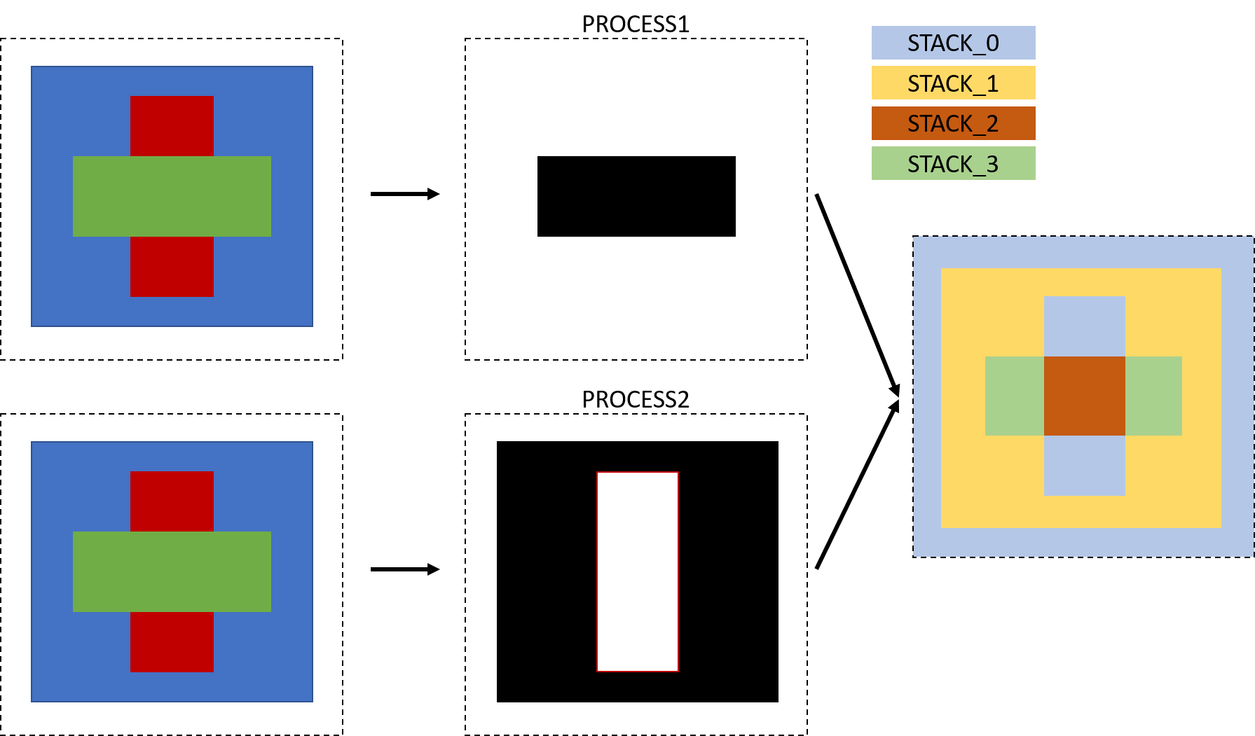
Assume the following example: we have a process which has 2 process layers:
PROCESS1, for which the mask is directly defined by LAYER1, and
PROCESS2, for which the mask is generated by the boolean xor between LAYER2 and LAYER3.
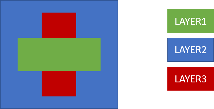
Layout of the structure to be virtually fabricated
We can write the process_layer_map as follows:
process_layer_map = {
    TECH.PROCESS.PROCESS1: TECH.PPLAYER.LAYER1,
    TECH.PROCESS.PROCESS2: TECH.PPLAYER.LAYER2 ^ TECH.PPLAYER.LAYER3
}
For the virtual fabrication, it does not matter whether the layers are i3.Layer or PPLayer objects.
These specified boolean operations defined will be used to create a final mask layer for each process:
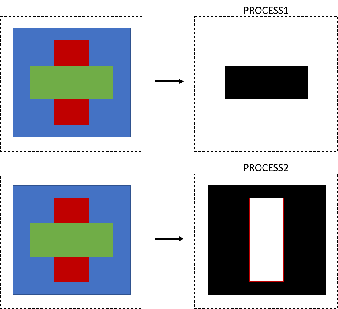
Final mask layers generated for each process layer
From mask layers to material stacks
The final mask layers are mapped to material stacks with a combination of two specifications:
process_to_material_stack_map: related combinations of final mask layers to a material stack (
i3.MaterialStack), where for every point in the layout there is a one (1) or a zero (0) for each final mask layer.is_lf_fabrication: specifies whether drawn areas on the final mask layer are 1 or 0.
If the corresponding entry is False, then a drawn shape on the final mask will be associated with a 1 in the process_to_material_stack_map table.
If the corresponding entry is True, then a drawn shape on the final mask will be associated with a 0 in the process_to_material_stack_map table.
TECH.VFABRICATION = TechnologyTree()
TECH.VFABRICATION.PROCESS_FLOW = VFabricationProcessFlow(
  active_processes=[
      TECH.PROCESS.PROCESS1,
      TECH.PROCESS.PROCESS2
  ],
  process_layer_map={
      TECH.PROCESS.PROCESS1: TECH.PPLAYER.LAYER1,
      TECH.PROCESS.PROCESS2: TECH.PPLAYER.LAYER2 ^ TECH.PPLAYER.LAYER3
  },
  process_to_material_stack_map=[
      ((0, 0), TECH.MATERIAL_STACKS.STACK_0),
      ((0, 1), TECH.MATERIAL_STACKS.STACK_1),
      ((1, 0), TECH.MATERIAL_STACKS.STACK_2),
      ((1, 1), TECH.MATERIAL_STACKS.STACK_3),
  ],
  is_lf_fabrication={
      TECH.PROCESS.PROCESS1: False,
      TECH.PROCESS.PROCESS2: False
  }
)
Note
The first entry in the process_material_stack_map is used as the default (background) material stack.
As illustrated below the masks are then combined to create virtually fabricated structure.
Mechanism used for the virtual fabrication.
Our samples contain an executable example on how to define a virtual fabrication and how visualize it or use it for cross sections.
It’s a good start to experiment with it to get a better understanding about its inner behavior.
You can find it at samples/technology/virtual_fabrication_example.py or download it here
# This is an advanced example on how to build Virtual Fabrication Process Flows.
# It's meant for PDK and library builders who want to include this process information
# in their technology. This way users of the PDK can with little effort export their
# components to 3rd party solvers.
import ipkiss3.all as i3
from ipkiss.visualisation.display_style import DisplayStyle
from ipkiss.visualisation import color
dummy_mat = i3.Material(name="dummy0_mat", epsilon=1, display_style=DisplayStyle(color=color.COLOR_SANGRIA))
# We'll have 4 material stacks
dummy_mstack0 = i3.MaterialStack(
name="dummy0", materials_heights=[(dummy_mat, 1.0)], display_style=DisplayStyle(color=color.COLOR_CHERRY)
)
dummy_mstack1 = i3.MaterialStack(
name="dummy1", materials_heights=[(dummy_mat, 2.0)], display_style=DisplayStyle(color=color.COLOR_DARK_GREEN)
)
dummy_mstack2 = i3.MaterialStack(
name="dummy2", materials_heights=[(dummy_mat, 3.0)], display_style=DisplayStyle(color=color.COLOR_GRAY)
)
dummy_mstack3 = i3.MaterialStack(
name="dummy3", materials_heights=[(dummy_mat, 0.5)], display_style=DisplayStyle(color=color.COLOR_MAGENTA)
)
# We'll use 3 Layers in our test structure
LAY0 = i3.Layer(0)
LAY1 = i3.Layer(1)
LAY2 = i3.Layer(2)
# and our technology uses 3 processes
PROCESS1 = i3.ProcessLayer(extension="ext1", name="dummyproc1")
PROCESS2 = i3.ProcessLayer(extension="ext2", name="dummyproc2")
PROCESS3 = i3.ProcessLayer(extension="ext3", name="dummyproc3")
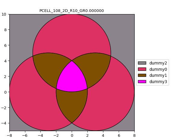
vfab_flow = i3.VFabricationProcessFlow(
active_processes=[PROCESS1, PROCESS2, PROCESS3],
process_layer_map={
# any of LAY0, LAY1 or LAY2 :
PROCESS1: LAY0 | LAY1 | LAY2,
# everwhere LAY1 or LAY2 :
PROCESS2: (LAY1 & LAY2) | (LAY1 & LAY0) | (LAY2 & LAY0),
# only when all layers are present:
PROCESS3: LAY0 & LAY1 & LAY2,
},
process_to_material_stack_map=[
((0, 0, 0), dummy_mstack2),
((1, 0, 0), dummy_mstack0), # mstack 0 where only 1 layer is present
((1, 1, 0), dummy_mstack1), # mstack 1 where any combination of 2 layers is present
((1, 1, 1), dummy_mstack3), # mstack 3 where all layers are present
],
is_lf_fabrication={
PROCESS1: False,
PROCESS2: False,
PROCESS3: False,
},
)
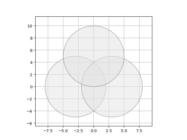
# We make a Venn - Diagram like teststructure
lay = i3.LayoutCell().Layout(
elements=[
i3.Circle(layer=LAY0, center=(-3, 0), radius=5.0),
i3.Circle(layer=LAY1, center=(3, 0), radius=5.0),
i3.Circle(layer=LAY2, center=(0, 5), radius=5.0),
]
)
# We visualize the layers
lay.visualize()
# visualize_2d displays a top down view of the fabricated layout
lay.visualize_2d(vfabrication_process_flow=vfab_flow)
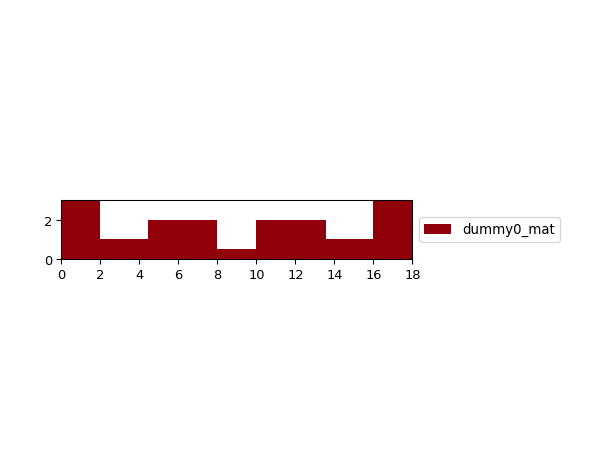
# we can also calculate and visualize the cross_section
lay.cross_section(i3.Shape([(-9, 3), (9, 3)]), process_flow=vfab_flow).visualize()
Traces
Contains the default settings for drawing traces such as waveguides and electrical traces. Three different trees need to be built.
TECH.TRACE
Contains the default settings for traces at the highest level. Those are often overridden by more specific settings.
# TRACES (Default settings for a default trace)
class TechTraceTree(DelayedInitTechnologyTree):
    def initialize(self):
        from ipkiss.primitives.layer import Layer

        self.DEFAULT_LAYER = Layer(0)
        self.CONTROL_SHAPE_LAYER = PPLayer(TECH.PROCESS.NONE, TECH.PURPOSE.TRACE)
        self.BEND_RADIUS = 5.0
        self.DRAW_CONTROL_SHAPE = False


TECH.TRACE = TechTraceTree()
TECH.PCELLS.WG
Contains the default waveguide template.
# Default waveguide template


class TechWgTree(DelayedInitTechnologyTree):
    def initialize(self):
        from picazzo3.traces.wire_wg.trace import WireWaveguideTemplate

        self.WIRE = WireWaveguideTemplate(name="WIRE_WG_TEMPLATE", library=TECH.PCELLS.LIB)
        self.WIRE.Layout(
            core_width=TECH.WG.WIRE_WIDTH, cladding_width=TECH.WG.CLADDING_WIDTH, core_process=TECH.PROCESS.WG
        )

        self.WIRE.CircuitModel(n_eff=2.86, n_g=2.86, center_wavelength=1.55, loss_dB_m=0.0)  # Default values

        from picazzo3.traces.rib_wg.trace import RibWaveguideTemplate, RibWireWaveguideTemplate

        self.RIB = RibWaveguideTemplate(name="RIB_WG_TEMPLATE", library=TECH.PCELLS.LIB)
        self.RIB.Layout(
            core_width=TECH.RWG.RIB_WIDTH, cladding_width=TECH.RWG.CLADDING_WIDTH, core_process=TECH.PROCESS.RWG
        )

        self.RIB.CircuitModel(n_eff=2.86, n_g=2.86, center_wavelength=1.55, loss_dB_m=0.0)  # Default values

        self.RIBWIRE = RibWireWaveguideTemplate(name="RIBWIRE_WG_TEMPLATE", library=TECH.PCELLS.LIB)
        self.RIBWIRE.Layout(
            core_width=TECH.RWG.RIB_WIDTH,
            strip_width=TECH.RWG.STRIP_WIDTH,
            cladding_width=TECH.RWG.CLADDING_WIDTH,
            core_process=TECH.PROCESS.RWG,
            strip_process=TECH.PROCESS.WG,
        )

        self.RIBWIRE.CircuitModel(n_eff=2.86, n_g=2.86, center_wavelength=1.55, loss_dB_m=0.0)  # Default values

        self.DEFAULT = self.WIRE


TECH.PCELLS.WG = TechWgTree()
TECH.PCELLS.METAL
Contains the default electrical wire template.
# Default templates for electrical wires.


class TechWireTree(DelayedInitTechnologyTree):
    def initialize(self):
        from picazzo3.traces.electrical_wire import ElectricalWireTemplate

        tpl = ElectricalWireTemplate(name="DEFAULT_WIRE_TEMPLATE", library=TECH.PCELLS.LIB)
        self.WIRE = tpl
        self.DEFAULT = self.WIRE


TECH.PCELLS.METAL = TechWireTree()
Grating Couplers
Here the grating coupler that are used in PICAZZO are defined. This is required to adapt the default fiber couplers used by IOFibcoup.
####################################################################
# DEFAULT FIBER COUPLER
####################################################################

from __future__ import division
from ipkiss.technology import get_technology
from ipkiss.technology.technology import TechnologyTree, DelayedInitTechnologyTree
import numpy as np

TECH = get_technology()
TECH.IO = TechnologyTree()
TECH.IO.DEFAULT_FIBCOUP_SPACING = 25.0  # Default spacing between fibercouplers for IOFibCoup


###########################################################
# Straight Gratings
###########################################################


class TechFibCoupTreeStraight(DelayedInitTechnologyTree):
    def initialize(self):
        self.SOCKET = TechnologyTree()
        self.SOCKET.LENGTH = 50.0
        self.SOCKET.WIDTH = 10.0

        from picazzo3.traces.wire_wg import WireWaveguideTemplate

        wide_trace_template = WireWaveguideTemplate()
        wide_trace_template.Layout(core_width=10.0, cladding_width=14.0)

        self.SOCKET.TRACE_TEMPLATE = wide_trace_template  # Wide trace template.

        # TE Grating
        self.GRATING_TE = TechnologyTree()
        self.GRATING_TE.N_O_LINES = 25  # Default number of lines used.
        self.GRATING_TE.PERIOD = 0.63  # Default period used in the grating.
        self.GRATING_TE.LINE_WIDTH = 0.315  # Default linewidth used in the grating.
        self.GRATING_TE.BOX_WIDTH = 14.0  # Default box width

        # TM Grating
        self.GRATING_TM = TechnologyTree()
        self.GRATING_TM.N_O_LINES = 16  # Default number of lines used.
        self.GRATING_TM.PERIOD = 1.080  # Default period used in the grating.
        self.GRATING_TM.LINE_WIDTH = 0.540  # Default linewidth used in the grating.
        self.GRATING_TM.BOX_WIDTH = 14.0  # Default box width

        # default
        self.GRATING = self.GRATING_TE


class TechFibcoupStraightCellsTree(DelayedInitTechnologyTree):
    def initialize(self):
        # standard gratings 1550nm
        def STANDARD_GRATING_1550_TE():
            from picazzo3.fibcoup.uniform import UniformLineGrating as _ULG

            t_tree = TECH.IO.FIBCOUP.STRAIGHT
            G = _ULG(name="std_grating_1550", trace_template=t_tree.SOCKET.TRACE_TEMPLATE, library=TECH.PCELLS.LIB)
            G.Layout(
                period=t_tree.GRATING.PERIOD,
                line_width=t_tree.GRATING_TE.LINE_WIDTH,
                line_length=t_tree.GRATING_TE.BOX_WIDTH,
                n_o_periods=t_tree.GRATING_TE.N_O_LINES,
            )
            TECH.PCELLS.LIB.add(G.dependencies())  # make sure that the child cells are also added to this lib
            return G

        # standard gratings 1550nm TM polarization
        def STANDARD_GRATING_1550_TM():
            from picazzo3.fibcoup.uniform import UniformLineGrating as _ULG
            from picazzo3.traces.wire_wg import WireWaveguideTemplate

            std1550_grating_trench = 0.540
            std1550_grating_period = 1.080
            std1550_grating_n_o_periods = 16
            wg_t = WireWaveguideTemplate(name="STD_FIBCOUP_SOCKET_WG_TM_T")
            wg_t.Layout(core_width=10.0, cladding_width=14.0)
            G = _ULG(name="std_grating_1550_tm", trace_template=wg_t, library=TECH.PCELLS.LIB)
            G.Layout(
                period=std1550_grating_period,
                line_width=std1550_grating_trench,
                n_o_periods=std1550_grating_n_o_periods,
            )
            TECH.PCELLS.LIB.add(G.dependencies())  # make sure that the child cells are also added to this lib
            return G

        self.DEFAULT_GRATING_TE = STANDARD_GRATING_1550_TE()
        self.DEFAULT_GRATING_TM = STANDARD_GRATING_1550_TM()
        self.DEFAULT_GRATING = self.DEFAULT_GRATING_TE


###########################################################
# Curved Gratings
###########################################################


class TechFibcoupTreeCurved(DelayedInitTechnologyTree):
    def initialize(self):
        # Socket
        self.SOCKET = TechnologyTree()
        self.SOCKET.LENGTH = 20.0
        self.SOCKET.STRAIGHT_EXTENSION = (0.0, 0.05)  # Default straight extentions used for the socket taper.
        self.SOCKET.MARGIN_FROM_GRATING = (
            TECH.WG.SHORT_STRAIGHT
        )  # Distance between the last grating line and the end of the socket by default
        self.SOCKET.START_TRACE_TEMPLATE = TECH.PCELLS.WG.DEFAULT
        self.SOCKET.TRANSITION_LENGTH = 5.0

        from picazzo3.traces.wire_wg import WireWaveguideTemplate

        wide_trace_template = WireWaveguideTemplate(name="LinearTransitionSocket_WGT")
        wide_trace_template.Layout(core_width=17.0, cladding_width=2 * TECH.WG.TRENCH_WIDTH + 17.0)

        self.SOCKET.WIDE_TRACE_TEMPLATE = wide_trace_template  # Wide trace template.

        # Grating

        self.GRATING = TechnologyTree()
        self.GRATING.PERIOD = 0.63  # Default period used in the grating.
        self.GRATING.FOCAL_DISTANCE = 20.0  # Default focal distance of curved gratings.
        self.GRATING.BOX_WIDTH = 15.5  # Default box width
        self.GRATING.N_O_LINES = int(np.floor(self.GRATING.BOX_WIDTH / self.GRATING.PERIOD))
        self.GRATING.START_RADIUS = (
            self.GRATING.FOCAL_DISTANCE - self.GRATING.BOX_WIDTH / 2.0
        )  # Default first radius of the grating.

        self.GRATING.ANGLE_SPAN = 90  # Default angle span of a curved grating when it is not boxed.


class TechFibcoupCurvedCellsTree(DelayedInitTechnologyTree):
    def initialize(self):

        from picazzo3.fibcoup.curved import FiberCouplerCurvedGrating

        # Creating the wire templates for the socket.
        t_tree = TECH.IO.FIBCOUP.CURVED
        fc_cell = FiberCouplerCurvedGrating(
            start_trace_template=t_tree.SOCKET.START_TRACE_TEMPLATE,
            wide_trace_template=t_tree.SOCKET.WIDE_TRACE_TEMPLATE,
            library=TECH.PCELLS.LIB,
        )
        fc_cell.Layout(
            period_x=t_tree.GRATING.PERIOD,  # We with a period of 0.8
            focal_distance_x=t_tree.GRATING.FOCAL_DISTANCE,  # We use a focal distance of 20.0
            # n_o_lines=t_tree.GRATING.N_O_LINES,# We set the number of lines to 30
            # min_x=t_tree.GRATING.START_RADIUS,
            box_width=t_tree.GRATING.BOX_WIDTH,  # All the lines will be contained between -20 and 20
            socket_straight_extension=t_tree.SOCKET.STRAIGHT_EXTENSION,
        )
        TECH.PCELLS.LIB.add(fc_cell.dependencies())  # make sure that the child cells are also added to this lib

        self.DEFAULT_GRATING = fc_cell


TECH.IO.FIBCOUP = TechnologyTree()
TECH.IO.FIBCOUP.CURVED = TechFibcoupTreeCurved()
TECH.IO.FIBCOUP.CURVED.PCELLS = TechFibcoupCurvedCellsTree()
TECH.IO.FIBCOUP.STRAIGHT = TechFibCoupTreeStraight()
TECH.IO.FIBCOUP.STRAIGHT.PCELLS = TechFibcoupStraightCellsTree()
TECH.IO.FIBCOUP.DEFAULT = TECH.IO.FIBCOUP.STRAIGHT


class TechAdapterTree(DelayedInitTechnologyTree):
    def initialize(self):
        self.IOFIBCOUP = TechnologyTree()
        self.IOFIBCOUP.FANOUT_LENGTH = 40.0
        self.IOFIBCOUP.S_BEND_ANGLE = 60.0
        self.IOFIBCOUP.CONNECT_TRANSITION_LENGTH = None  # automatic
        self.IOFIBCOUP.FIBER_COUPLER_TRANSITION_LENGTH = None  # automatic

        self.DEFAULT_ADAPTER = self.IOFIBCOUP


class TechIoFibcoupAdapterPCellTree(DelayedInitTechnologyTree):
    def initialize(self):
        from picazzo3.container.iofibcoup import IoFibcoup

        self.ADAPTER = IoFibcoup


TECH.IO.ADAPTER = TechAdapterTree()
TECH.IO.ADAPTER.IOFIBCOUP.PCELLS = TechIoFibcoupAdapterPCellTree()
OpenAccess (Link for Siemens EDA only)
IPKISS can export a database to OpenAccess. This database can then be used inside other EDA tools supporting OpenAccess.
Layer settings
Layer settings for the OpenAccess database are in the TECH.OPENACCESS settings tree. OpenAccess uses similar concepts as IPKISS, hence a one-to-one map between the two is easily made.
IPKISS Concept |
OpenAccess concept |
|---|---|
ProcessLayer |
oaPhysicalLayer |
PatternPurpose |
oaPurpose |
PPLayer |
LayerPurposePair (LPP) extension - not in standard OA |
When using Link for Siemens EDA, the following TECH keys need to be set up:
TECH.OPENACCESS.EXPORT_LAYER_MAP: map of ProcessLayer to an oaPhysicalLayer number which will be used to identify the Layer
TECH.OPENACCESS.EXPORT_PURPOSE_MAP: map of PatternPurpose to an oaPurpose number which will be used to identify the Purpose. Note that OpenAccess has a number of reserved purposes.
TECH.OPENACCESS.FILTER: IPKISS Filter which will be applied to each object exported to OpenAccess. This allows to have the same data exported to OpenAccess (e.g. cut polygons) as to GDSII (or differently, if desired).
Hence, the mapping between IPKISS and OpenAccess is always done for Layers and for Purposes separately, unlike for GDSII where it is possible to map any (ProcessLayer, PatternPurpose) pair onto any (GDSII layer, GDSII datatype) pair. The PPLayer to LPP mapping is made implicitly and cannot be altered.
Note
OpenAccess has a number of reserved purpose numbers. In particular, the default one considered by Link for Siemens EDA is the drawing purpose, used for normal ‘drawn’ mask data. The PatternPurpose which maps to the drawing purpose should not be specified in TECH.OPENACCESS.EXPORT_PURPOSE_MAP.
Also note that, because of this, it is not generally possible to use identical numbers for IPKISS PatternPurpose / OpenAccess oaPurpose / GDSII datatype, unless the drawing purpose is not used.
Routing settings
A TECH.ROUTING.WAVEGUIDE_GENERATION_GUIDE_LAYERS is defined which contains a mapping from routing layers to
waveguide generation functions. For example:
# In technology/openaccess.py
TECH = get_technology()


class RoutingTechTree(DelayedInitTechnologyTree):
    def initialize(self):
        self.WAVEGUIDE_GENERATION_GUIDE_LAYERS = {
            TECH.PPLAYER.WG.TRACE: generate_strip_wg,
            TECH.PPLAYER.RIB.TRACE: generate_rib_wg,
        }


TECH.ROUTING = RoutingTechTree()
Here, generate_strip_wg and generate_rib_wg are functions that generate the waveguide.
A waveguide function takes the start port, end port, and shape as input,
and outputs a (possibly modified) shape, and the waveguide itself.
Below is an example:
# in technology/openaccess.py

def generate_strip_wg(start_port, end_port, shape):
    """Generate a strip waveguide.

    Parameters
    ----------
    start_port: i3.Port or None
        The starting port. If the user connects the starting point of the shape to a device,
        then it contains that port.
        If the starting point is not physically connected to a device in the layout, then start_port=None.
    end_port: i3.Port or None
        Same, for the ending point of the shape.
    shape: i3.Shape
        Shape the user has drawn, which defines the control points of the waveguide.
        If only two points are given and start_port and end_port are given, it means the user expects
        a valid drawn route between these two ports. This means the shape needs to be updated
        (for example, a manhattan route).

    Returns
    -------
    shape: i3.Shape
        The shape (possibly modified from the original)
    waveguide: i3.PCell
        The generated waveguide

    """
    from ipkiss3.pcell.routing.manhattan import RouteManhattan
    from ipkiss3.pcell.photonics.rounded_waveguide import RoundedWaveguide

    if len(shape) == 2 and not start_port is None and not end_port is None:
        # User wants to auto-route this waveguide between two ports
        # RouteManhattan uses the technology defaults - update when needed
        shape = RouteManhattan(input_port=start_port, output_port=end_port)

    cell_params = {}
    if start_port is not None:
        cell_params['trace_template'] = start_port.trace_template
    elif end_port is not None:
        cell_params['trace_template'] = end_port.trace_template

    wg = RoundedWaveguide(**cell_params)
    layout = wg.Layout(shape=shape)
    return shape, wg
The waveguide generation function calculates how a waveguide is generated along a given shape. If the start and end port are given, that means the user wants to connect between two ports. If the user has drawn a straight line between these two ports, it means the user expects the waveguide function to recalculate the shape.
How to use these waveguide routes from an EDA tool is explained in Step 3: Route and generate waveguides.
Required Technology Keys: IPKISS
IPKISS requires a number of technology keys to be defined in order for all the parts of ipkiss to work. Even if some of them have no meaning for your technology, you will still need to define them and provide some value for them when defining your own technology.
Name generation
The name generator is used to automatically calculate a name for each cell, if a name is not given during initialization. By default, it causes pcells to get the PCELL_ name prefix, and counting starts at 0. If _name_prefix is defined in your pcell, that will be used for the prefix, instead.
TECH.ADMIN.NAME_GENERATOR: Name generator for your PCells.
TECH.ADMIN.NAME_GENERATOR_I24: Name generator used in the for ipkiss2.4 structures.
Discretization metrics
These values affect how the output of the layout is generated.
TECH.METRICS.ANGLE_STEP: Angle step (in degrees) used for discretization of bends.
TECH.METRICS.GRID: Discretization of the grid GDSII file (in meter).
TECH.METRICS.UNIT: Unit of the GDSII file (in meter).
Port properties
An optical port is exported with a box drawn on DEFAULT_LAYER. The box dimensions are (TECH.PORT.DEFAULT_LENGTH, self.width)
TECH.PORT.DEFAULT_LAYER: Default layer used for ports.
TECH.PORT.DEFAULT_LENGTH: Default length used for ports.
Generic trace properties.
TECH.TRACE.BEND_RADIUS: Default bend radius, used during automatic routing.
TECH.TRACE.DRAW_CONTROL_SHAPE: Turn on/off the drawing of a control shape.
TECH.TRACE.CONTROL_SHAPE_LAYER: Layer used for the drawing of the control shape.
TECH.TRACE.DEFAULT_LAYER: Default layer used of the drawing of shapes.
Default model parameters
TECH.DEFAULT_WAVELENGTH: Default wavelength used for waveguide models.
TECH.WG_DEFAULTS.N_EFF: Default n_eff for waveguide models.
TECH.WG_DEFAULTS.N_GROUP: Default group index used for waveguide models.
TECH.WG_DEFAULTS.LOSS_DB_PERM: Default loss per m in dB used for waveguide models.
Default waveguide parameters.
TECH.WG_DEFAULTS.CORE_LAYER: Default core layer used in waveguides.
TECH.WG.SPACING: Default waveguide spacing used in adaptors.
TECH.WG.WIRE_WIDTH: Default wire width (needed for backward compatibility).
TECH.WG.EXPANDED_TAPER_LENGTH: Default length of an extended taper for extended waveguides.
TECH.WG.EXPANDED_WIDTH: Default width of expanded waveguides.
TECH.WG.TRENCH_WIDTH: Default width of a trench of a wavguide.
Used during routing.
TECH.WG.SHORT_STRAIGHT: Default minimum length required for any of the straight sections in a route.
TECH.WG.EXPANDED_STRAIGHT: Default length of an expanded straight waveguide.
TECH.PROCESS.WG: Default process for waveguides.
TECH.PROCESS.NONE: Default process for things that are not added to the GDSII.
TECH.PPLAYER.M1.LINE: Default layer for M1 guides.
TECH.PPLAYER.M2.LINE: Default layer for M2 guides.
TECH.PPLAYER.V12.PILLAR: Default layer for M12 vias.
TECH.PPLAYER.WG.TEXT: Default layer for text on a design.
TECH.PPLAYER.ERROR.GENERIC: Default layer for drawing errors.
TECH.PCELLS.WG.DEFAULT: Default waveguide template for this technology.
TECH.PCELLS.LIB: Default PCELL library.
TECH.PCELLS.METAL.DEFAULT: Default Metal trace template.
TECH.METAL.DEFAULT_PROCESS: Default process used for metals.
TECH.METAL.LINE_WIDTH: Default width of metal traces.
TECH.VIAS.DEFAULT.TOP_SHAPE: Default top_shape of a via.
TECH.VIAS.DEFAULT.BOTTOM_SHAPE: Default bottom_shape of a via.
TECH.VIAS.DEFAULT.VIA_SHAPE: Default pillar shape of a via.
GDS export settings.
These affect how your designs are exported to GDS.
The default EXPORT_LAYER_MAP and IMPORT_LAYER_MAP automatically convert IPKISS layers to a gds
number/datatype and vice versa (through AutoGdsiiLayerOutputMap
/ AutoGdsiiLayerInputMap).
This is in general not very useful as you want to have control over how the layers are exported.
The best way to do this is to define a layer map manually, and use
GenericGdsiiPPLayerOutputMap and
GenericGdsiiPPLayerInputMap.
TECH.GDSII.MAX_NAME_LENGTH: Max name length of a cell in char.
TECH.GDSII.EXPORT_LAYER_MAP: GDSII export layer map.
TECH.GDSII.IMPORT_LAYER_MAP: GDSII import layer map.
TECH.GDSII.NAME_FILTER: Filter applied on the names of the PCells before being exported to GDSII.
TECH.GDSII.MAX_VERTEX_COUNT: Max number of vertices in a polygon shape. Splitted otherwise.
TECH.GDSII.FILTER: List of filters applied to your PCells before export to GDSII.
TECH.GDSII.MAX_PATH_LENGTH: Max path length of the GDSII file. Splitted otherwise.
TECH.GDSII.STRNAME_CHARACTER_DICT: Dict for the mapping of illegal characters on legal. Applied to all cell names.
TECH.GDSII.STRNAME_ALLOWED_CHARACTERS: All allowed characters in a cell name.
Blocks
Blocks are the basic elements added to IoColumn. Below are default values for the spacing and width of the blocks.
TECH.BLOCKS.DEFAULT_YSPACING: Default spacing between blocks.
TECH.BLOCKS.DEFAULT_WIDTH: Default width of a block.
The default adapter (i.e., A PCell that ‘adapts’ or ‘wraps’ another PCell in an IoBlock to fit it into an IoColumn):
TECH.IO.ADAPTER.DEFAULT_ADAPTER.PCELLS.ADAPTER: Default adapter for I/O blocks.
Drawing purposes
TECH.PURPOSE.BBOX: Purpose for the bounding boxes.
TECH.PURPOSE.LF_AREA: Purpose for light field areas.
TECH.PURPOSE.LF.LINE: Purpose for light field lines.
TECH.PURPOSE.DF.LINE: Purpose for dark field areas.
TECH.PURPOSE.TEXT: Purpose for text.
Visualization
TECH.DISPLAY.DEFAULT_DISPLAY_STYLE_SET: Default display set for visualization in IPKISS.
Transitions
The AUTO_TRANSITION_DATABASE consists of a list of valid transitions (tapers). During automatic routing, if transitions have to be added between two given trace templates (e.g., rib and strib waveguide), the AUTO_TRANSITION_DATABASE is used to look up whether there is a valid transition between both.
TECH.PCELLS.TRANSITION.AUTO_TRANSITION_DATABASE: Default autotransition database.
Errors
TECH.PPLAYER.ERROR.CROSSING: error layer to indicate crossing waveguides
TECH.PPLAYER.ERROR.GENERIC: error layer to indicate other errors
Required Technology Keys: PICAZZO
In order to make the PICAZZO pcell library work on your technology, a set of technology keys are required as well.
Containers
TECH.CONTAINER.TERMINATE_PORTS.CHILD_SUFFIX: Suffix that will be added to the children of
TerminatePorts.TECH.CONTAINER.TERMINATE_PORTS.TERMINATION_INSTANCE_PREFIX: Suffix that will be added to the instances of the termination cells in
TerminatePorts.
Fiber couplers and IoFibcoup adapters
These provide default values for the parameters of IoFibcoup and
the picazzo fiber couplers.
TECH.IO.ADAPTER.IOFIBCOUP.CONNECT_TRANSITION_LENGTH: default length of the transition between the ‘fanout’ section and the straight connection traces to the fiber coupler in IoFibcoup.
TECH.IO.ADAPTER.IOFIBCOUP.FANOUT_LENGTH: default length of the ‘fanout’ section in IoFibcoup.
TECH.IO.ADAPTER.IOFIBCOUP.FIBER_COUPLER_TRANSITION_LENGTH: default transition length to the fiber coupler in IoFibcoup.
TECH.IO.ADAPTER.IOFIBCOUP.S_BEND_ANGLE: maximum s-bend angle to use in IoFibcouop.
TECH.IO.FIBCOUP.CURVED.SOCKET.MARGIN_FROM_GRATING: margin behind the grating before the coupler socket ends.
TECH.IO.FIBCOUP.CURVED.GRATING.ANGLE_SPAN: default angular span of curved grating.
TECH.IO.FIBCOUP.CURVED.GRATING.BOX_WIDTH: default box width of curved grating.
TECH.IO.FIBCOUP.CURVED.GRATING.FOCAL_DISTANCE: default focal distance of curved grating.
TECH.IO.FIBCOUP.CURVED.GRATING.N_O_LINES: default number of grating lines of curved grating.
TECH.IO.FIBCOUP.CURVED.GRATING.PERIOD: default period of curved grating.
TECH.IO.FIBCOUP.CURVED.GRATING.START_RADIUS: default radius of the first grating line of curved grating.
TECH.IO.FIBCOUP.CURVED.PCELLS.DEFAULT_GRATING: default curved grating cell.
TECH.IO.FIBCOUP.CURVED.SOCKET.LENGTH: default socket length.
TECH.IO.FIBCOUP.CURVED.SOCKET.START_TRACE_TEMPLATE: default start trace template of curved grating socket.
TECH.IO.FIBCOUP.CURVED.SOCKET.STRAIGHT_EXTENSION: default straight extension of curved grating behind the grating socket.
TECH.IO.FIBCOUP.CURVED.SOCKET.WIDE_TRACE_TEMPLATE: default end trace template of curved grating socket.
TECH.IO.FIBCOUP.DEFAULT.PCELLS.DEFAULT_GRATING: default grating coupler.
TECH.IO.FIBCOUP.DEFAULT.SOCKET.LENGTH: Default property value for curved grating couplers.
TECH.IO.FIBCOUP.STRAIGHT.GRATING.BOX_WIDTH: default box width of straight grating.
TECH.IO.FIBCOUP.STRAIGHT.GRATING.LINE_WIDTH: default linewidth of straight grating.
TECH.IO.FIBCOUP.STRAIGHT.GRATING.N_O_LINES: default number fo periods of straight grating.
TECH.IO.FIBCOUP.STRAIGHT.GRATING.PERIOD: default period of straight grating.
TECH.IO.FIBCOUP.STRAIGHT.PCELLS.DEFAULT_GRATING_TM: default TM grating.
TECH.IO.FIBCOUP.STRAIGHT.SOCKET.LENGTH: default socket length of straight grating.
TECH.IO.FIBCOUP.STRAIGHT.SOCKET.TRACE_TEMPLATE: default trace template of straight grating.
Modulators
These provide default values for the parameters of LateralPNPhaseShifterTemplate
and py:class:LongitudinalPNPhaseShifterTemplate<picazzo3.modulators.phase.trace.LongitudinalPNPhaseShifterTemplate>
TECH.MODULATORS.PHASESHIFTER.LATPN.BRIDGE_PITCH
TECH.MODULATORS.PHASESHIFTER.LATPN.BRIDGE_WIDTH
TECH.MODULATORS.PHASESHIFTER.LATPN.JUNCTION_OFFSET
TECH.MODULATORS.PHASESHIFTER.LONGPN.N_LENGTH
TECH.MODULATORS.PHASESHIFTER.LONGPN.N_WIDTH
TECH.MODULATORS.PHASESHIFTER.LONGPN.P_LENGTH
TECH.MODULATORS.PHASESHIFTER.LONGPN.P_WIDTH
TECH.MODULATORS.PHASESHIFTER.PN.JUNCTION_OVERLAP
TECH.MODULATORS.PHASESHIFTER.PN.NPLUS_EXTENSION
TECH.MODULATORS.PHASESHIFTER.PN.NPLUS_OFFSET
TECH.MODULATORS.PHASESHIFTER.PN.NPLUS_WIDTH
TECH.MODULATORS.PHASESHIFTER.PN.N_CONT_OFFSETS
TECH.MODULATORS.PHASESHIFTER.PN.N_CONT_PITCH
TECH.MODULATORS.PHASESHIFTER.PN.N_METAL1_OFFSET
TECH.MODULATORS.PHASESHIFTER.PN.N_METAL1_WIDTH
TECH.MODULATORS.PHASESHIFTER.PN.N_SIL_EXTENSION
TECH.MODULATORS.PHASESHIFTER.PN.N_SIL_OFFSET
TECH.MODULATORS.PHASESHIFTER.PN.N_SIL_WIDTH
TECH.MODULATORS.PHASESHIFTER.PN.N_WIDTH
TECH.MODULATORS.PHASESHIFTER.PN.PPLUS_EXTENSION
TECH.MODULATORS.PHASESHIFTER.PN.PPLUS_OFFSET
TECH.MODULATORS.PHASESHIFTER.PN.PPLUS_WIDTH
TECH.MODULATORS.PHASESHIFTER.PN.P_CONT_OFFSETS
TECH.MODULATORS.PHASESHIFTER.PN.P_CONT_PITCH
TECH.MODULATORS.PHASESHIFTER.PN.P_METAL1_OFFSET
TECH.MODULATORS.PHASESHIFTER.PN.P_METAL1_WIDTH
TECH.MODULATORS.PHASESHIFTER.PN.P_SIL_EXTENSION
TECH.MODULATORS.PHASESHIFTER.PN.P_SIL_OFFSET
TECH.MODULATORS.PHASESHIFTER.PN.P_SIL_WIDTH
TECH.MODULATORS.PHASESHIFTER.PN.P_WIDTH
waveguides
TECH.PCELLS.WG.RIB: Default ‘rib’ waveguide template
TECH.PCELLS.WG.RIBWIRE: Default ‘ribwire’ waveguide template
TECH.PCELLS.WG.WIRE: Default ‘wire’ waveguide template
PPLayers, ProcessLayers and PatternPurposes
TECH.PPLAYER.FC.TRENCH: Default fiber coupler trench layer
TECH.PPLAYER.N.LINE: Default N implant layer
TECH.PPLAYER.P.LINE: Default P implant layer
TECH.PPLAYER.NONE.DOC: Default documentation layer
TECH.PPLAYER.WG.CLADDING: Default waveguide cladding layer
TECH.PPLAYER.WG.CORE: Default waveguide core layer
TECH.PPLAYER.WG.TRENCH: Default waveguide trench layer
TECH.PROCESS.CON: Default contact hole process
TECH.PROCESS.FC: Default fiber coupler grating process
TECH.PROCESS.HFW: Default HF etch window process (oxide removal)
TECH.PROCESS.M1: Default metal1 process
TECH.PROCESS.M2: Default metal2 process
TECH.PROCESS.N: Default N implant process
TECH.PROCESS.P: Default P implant process
TECH.PROCESS.NPLUS: Default N++ implant process
TECH.PROCESS.PPLUS: Default P++ implant process
TECH.PROCESS.RWG: Default rib waveguide process
TECH.PROCESS.SIL: Default silicide process
TECH.PROCESS.SK: Default socket waveguide process
TECH.PROCESS.V12: Default via12 process
TECH.PURPOSE.DF.POLYGON: Default dark-field polygon drawing purpose
TECH.PURPOSE.DF_AREA: Default dark-field area drawing purpose
TECH.PURPOSE.DRAWING: Default drawing purpose
Rules
TECH.RWG.CLADDING_WIDTH: Default rib waveguide cladding width
TECH.RWG.RIB_WIDTH: Default rib waveguide rib width (shallow part)
TECH.RWG.STRIP_WIDTH: Default rib waveguide strip core width
TECH.SK.CLADDING_WIDTH: Default socket waveguide cladding width
TECH.TECH.MINIMUM_LINE: Overall minimum linewidth
TECH.TECH.MINIMUM_SPACE: Overall minimum spacing
TECH.VIAS.CONTACT_HOLE.M1_WIDTH: Default metal1 width on contact hole
TECH.VIAS.CONTACT_HOLE.PCELLS.DEFAULT_VIA: Default contact hole cell
TECH.VIAS.CONTACT_HOLE.SIL_WIDTH: Default silicide width on contact hole
TECH.VIAS.CONTACT_HOLE.VIA_WIDTH: Default via width on contact hole
TECH.VIAS.V12.M1_WIDTH: Default metal1 width on via12
TECH.VIAS.V12.M2_WIDTH: Default metal2 width on via12
TECH.VIAS.V12.N_O_SIDES: Default number of sides on via12 polygon
TECH.VIAS.V12.PCELLS.DEFAULT_VIA: Default default via12 cell
TECH.VIAS.V12.VIA_WIDTH: Default width of via12
TECH.WG.BEND_RADIUS: Default waveguide bend radius
TECH.WG.CLADDING_WIDTH: Default strip waveguide cladding width
TECH.WG.DC_SPACING: Default strip waveguide directional coupler spacing
TECH.WG.SHORT_TRANSITION_LENGTH: Default length of transitions
TECH.WG.SLOT_WIDTH: Default slot width for slot waveguides