Waveguides
This section gives an overview of the waveguide concepts in Ipkiss, and how to use waveguides in a design.
Waveguides are cells
In IPKISS, optical waveguides are not just drawings, but are full parametric cells that work and behave like any other PCell.
This provides a number of benefits:
Waveguides are parametrized and one can control their parameters (shape, bend radius, …) from within IPKISS (Link for Siemens EDA GUI or Python script).
Waveguides can be modeled by physical simulations (e.g. mode propagation tools or FDTD) as well as included in circuit simulations in the same fashion as other PCells.
Therefore, waveguides will typically be child cells of larger circuits.
Waveguides are Traces
The concept of waveguides is based on that of Traces. See reference: traces for reference documentation on this. A Trace connects multiple locations on the chip. Optical waveguides are traces in the optical domain, but there can be traces for electrical wiring, RF waveguides, fluidics, and so forth.
Trace Templates
IPKISS decouples the general properties of a trace (or waveguide) from its actual planar shape.
A trace template (or waveguide template in the case of optical waveguides) defines several aspects that govern how the waveguide is formed or extruded along its run length:
how the waveguide is drawn (Layout) along the shape of the waveguide,
the simulation model, e.g. effective index and group index of the waveguide,
and the geometrical cross-section, can be derived from the layout through virtual fabrication.
For this reason, many parametric cells in ipkiss take one or multiple trace_template parameters, which determines the template(s) of the waveguides that are part of that pcell.
Reference documentation for the different basic trace and trace template classes in ipkiss is in reference: traces.
Predefined waveguide templates
The picazzo pcell library contains a number of predefined waveguide templates for wire waveguides (fully etched), rib waveguides (partially etched), slot waveguides, thinned waveguides, and so forth. See picazzo reference: traces for more information.
How to use waveguides in a circuit (IPKISS)
In IPKISS python script, waveguides can be used in a (sub)circuit in various ways:
The
Circuitdefines the waveguides based on route and placement specifications that are provided by the user. The :py:class: ~ipkiss3.pcell.circuit.Circuit can also be used for workflows that need e.g. coupling between the instances, placement, routing and port specifications, by inheriting from this class and providing a more complex behavior in_default_instances,_default_specs, and_default_exposed_portsmethods.The user can manually add waveguides to a custom defined pcell in both layout and circuit simulation. See for example the advanced layout tutorial for introductory material on this.
How to use waveguides in a circuit (Link for Siemens EDA module)
From the L-Edit GUI, waveguides can be generated by first defining their route and then by executing ‘Generate All Waveguides’ from the Luceda menu. A waveguide cell will be instantiated for every waveguide route defined, but the user can still finetune the parameters of the waveguide, such as the bend radius and the shape.
See step 3 of the PDK-based design tutorial (route and generate waveguides).
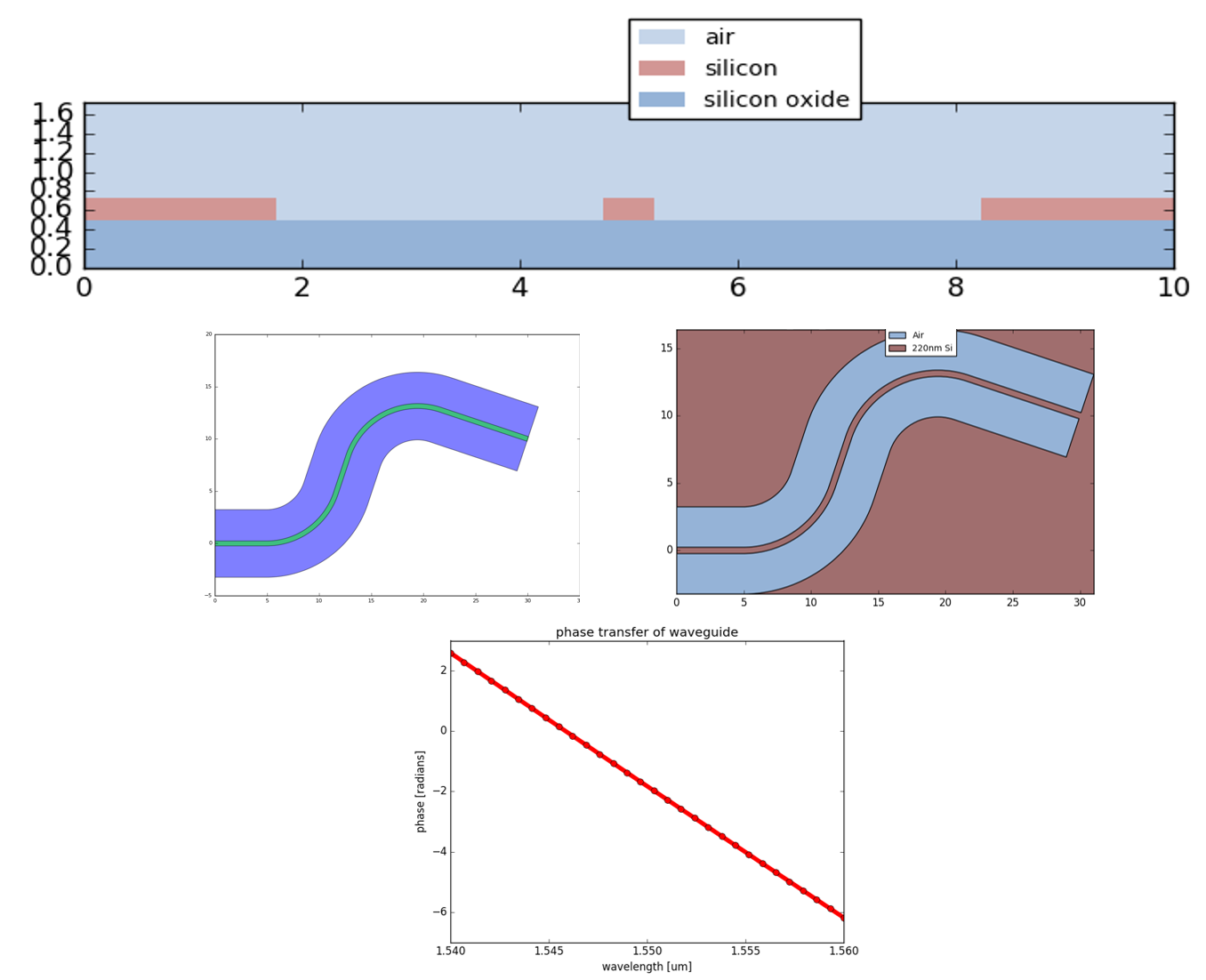
Basic waveguide example
Here is a basic example demonstrating the concepts above:
import si_fab.all as pdk
from ipkiss3 import all as i3
from picazzo3.traces.wire_wg.trace import WireWaveguideTemplate
import numpy as np
import pylab as plt

# waveguide template: wire waveguide from picazzo
# the template defines the cross-section: how it is drawn and what the simulation model properties are
wg_template = WireWaveguideTemplate(name="example_wire_template")
wg_template.Layout(core_width=0.47,
                   cladding_width=2 * 3.0 + 0.47,
                   core_process=i3.TECH.PROCESS.WG)
wg_t_cm = wg_template.CircuitModel(n_eff=2.4, n_g=4.5)

# waveguide: is extruded form the trace template along a given shape
wg = i3.RoundedWaveguide(name="example_wire_waveguides",
                         trace_template=wg_template)
# layout
layout = wg.Layout(shape=[(0.0, 0.0), (10.0, 0.0), (15.0, 15.0), (30.0, 10.0)],
                           bend_radius=7.0)

layout.visualize()

# virtual fabrication: top-down and cross-section views
layout.visualize_2d()
layout.cross_section(cross_section_path=i3.Shape([(0.0, -5.0), (0.0, 5.0)])).visualize()

# obtain and plot S21
# use a simulation model from layout to take the actual length as on the layout into account.
cm = wg.CircuitModel()
wavelengths=np.linspace(1.54, 1.56, 30)
S = cm.get_smatrix(wavelengths=wavelengths)

plt.figure()
plt.plot(wavelengths, np.unwrap(np.angle(S["in", "out"])), 'ro-', linewidth=5, markersize=7)
plt.xlabel('wavelength [um]')
plt.ylabel('phase [radians]')
plt.xlim([wavelengths[0], wavelengths[-1]])
plt.title('phase transfer of waveguide')
plt.show()
As a result, the several outputs are plotted: layout, cross-section, top-down material view and S-parameters (phase of S21 plotted).