AWG Simulation
In this guide we explain the workflow of an AWG simulation, starting from a high-level simulation strategy, which we then break down into different pieces. We also emphasize the parameters that have the largest influence on the simulation results, so that you can easily make design variations and study the impact of different design choices.
High-level AWG simulation strategy
The exact AWG topology doesn’t matter for the high-level simulation strategy, and for the remainder of this guide we will consider an AWG with 1 input and M outputs (1 -> M AWG), together with N grating arms. A schematic image is shown below.

An AWG conceptually contains three parts, which are outlined below. Since each of these parts is passive, we can represent them with a wavelength-dependent S-matrix. The S-matrices can be further combined (using our circuit simulator Caphe) in order to retrieve a complete model.
Component |
Simulation strategy |
|---|---|
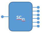
Input star coupler 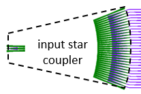
|
The (1+N)x(1+N) S-matrix is simulated by simulating the apertures and the slab region: Star coupler simulation |
Waveguide array 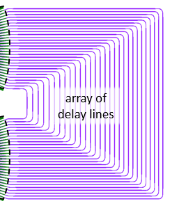
|
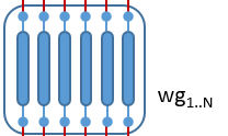
The waveguide array is simulated by simulating the individual waveguides using a model provided by the foundry / PDK (or optionally your own waveguide models). Waveguide array simulation |
Output star coupler 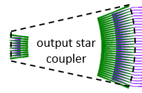
|
The (M+N)x(M+N) S-matrix is simulated by simulating the apertures and the slab region: Star coupler simulation |
Star coupler simulation
The star coupler simulation consists of two parts: the aperture and the star coupler region. After both are simulated, we construct the S-parameters of the star coupler using modal overlaps.
Simulation of the apertures
For the apertures, we want to know two things:
the transmission as a function of wavelength, and
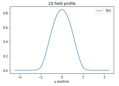
the aperture field profile, which is used as slab excitation
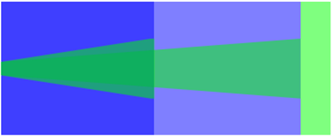
Aperture Layout |
Simulation (default: camfr) |
Aperture field profile |
|---|---|---|
|
|
|
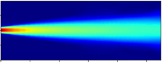
The simulation is by default performed with CAMFR. In this case, it does 1D mode solving, and 2D EME (eigenmode expansion) propagation. At the end of the aperture, light enters the FPR (Free Propagation Region) with a certain field profile (rightmost picture above). The aperture field profile is calculated by expanding the output of the mode profile of the aperture into the slab modes (this could e.g. lead to losses due to vertical mode mismatch).
Note: the field profile is also used to calculate the spreading angle. The diffraction angle is a parameter of the design algorithm.
Parameters that impact the simulation of the aperture
By default, camfr is used to calculate the aperture transmission and the field profile (
awg_designer.all.OpenWireWgAperture.FieldModelFromCamfr). This simulation is done directly from the layout, which means that the change in the aperture layout will impact the simulation.When using camfr: the simulation window and camfr simulation settings are parameters that influence the final field profile.
Note: you can specify your own field profile using
awg_designer.all.OpenWireWgAperture.FieldModelFromFunction.
Overestimation of transmission power
The amount of light that is collected at the end of the aperture depends on its collection width.
For a SingleAperture, this is determined by the width property of FieldModelFromCamfr.
If this value is too large, it is possible for the collection window of the output apertures to overlap with those of adjacent apertures belonging to the same star coupler, which is currently unsupported by AWG Designer
This causes the same propagated light from the slab region to be counted multiple times when calculating the overlap between the light in the slab region and the aperture field profile.
This thus leads to an overestimation of the transmission power at the outputs of the star coupler.
To avoid this, it is recommended to have a collection width equal to the separation (centre-to-centre) between the apertures at the center of the array of apertures.
Note that the aperture separation for the input/output apertures and for the waveguide apertures is generally different with the former being much larger.
For this reason, users are advised to instantiate different aperture objects for the apertures of the waveguide array and the input/output apertures that differ in the width property of their FieldModelFromCamfr view.
Note that this overestimation does not affect the shape of the field profile of the collected light.
Simulation of the star coupler region
The aperture field profile is launched into the star coupler region. Luceda AWG Designer uses Rayleigh-Sommerfeld diffraction to propagate through the slab region, an algorithm that is formulated for 2D, and is accurate for wide-angle slabs. Currently there are no roundtrips simulated; only a single pass is done.
Star coupler S-parameter calculation using mode overlaps
Modal overlaps are used for measuring the field overlap and power coupling between an input mode from one port and all of the modes of a second port. The fields are evaluated at the output side of the star coupler, where we calculate the modal overlap between the propagated fields and the field profile of the output apertures.
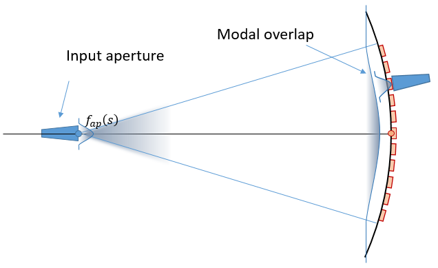
Calculating the modal overlap between the field at the output of the star coupler and the field profile of an output aperture.
The output of this modal overlap determines the complex-valued transmission from the mode at the inset of the star coupler (from the input aperture) to the mode at the output of the star coupler. We then account for the complex-valued transmission of the apertures themselves to end up with the final S-parameter values of the full star coupler (including apertures).
Parameters that impact the simulation of the star coupler
Aperture field profile: the exact field profile shape has a large impact on the final simulation result. This field propagates through the FPR, and on the other side, modal overlaps are performed between the propagated field and the field profiles of the output apertures. Hence, the field profile has a significant impact on the shape of the AWG transmission (this is easy to see when you use MMI input apertures, which are typically used to design flat-top filter characteristics).
The loss in the aperture has an impact on the overall AWG transmission.
The slab material index: this determines the propagation through the slab. Either there are defined manually (
awg_designer.all.SlabTemplate.SlabModes), or simulated with camfr (awg_designer.all.SlabTemplate.SlabModesFromCamfr). When designing the AWG, the position of the output apertures depends on the slab effective index (seeawg_designer.all.get_angles_out()).
Waveguide array simulation
The waveguides are simulated individually using the models provided by the PDK which you are using. There is currently no cross-talk simulated between the waveguides.
In most cases, waveguides are described analytically using a phase propagation which is determined by the length of the waveguide, the wavelength-dependent effective index \(n_{eff}(\lambda)\) and a loss parameter (which might be wavelength-dependent).
Some models may include phase errors caused by variations of thickness, width or refractive index along the waveguide. In that case, the simulation results will clearly show that the crosstalk levels go up - indeed, AWG devices are very sensitive to the waveguide quality (and for that reason, in certain AWG configurations, the waveguide widths are expanded in the straight sections in order to reduce loss and phase errors).
Please check the IPKISS manual delivered with the foundry handbook to read more about how the waveguides are modeled.
In case you may want to write your own waveguide models, you can check out the SiFab library as a reference and check the documentation on how to build compact models.
Parameters that impact the simulation of the waveguides
The waveguide wavelength-dependent effective index: \(n_{eff}(\lambda)\).
The way the waveguides are constructed: we use TaperedWaveguide to segment the waveguide into different pieces, each of them comes with its own compact model.