Getting started with the Luceda AWG Designer
Here’s a schematic overview. The steps are explained in more detail below the picture.
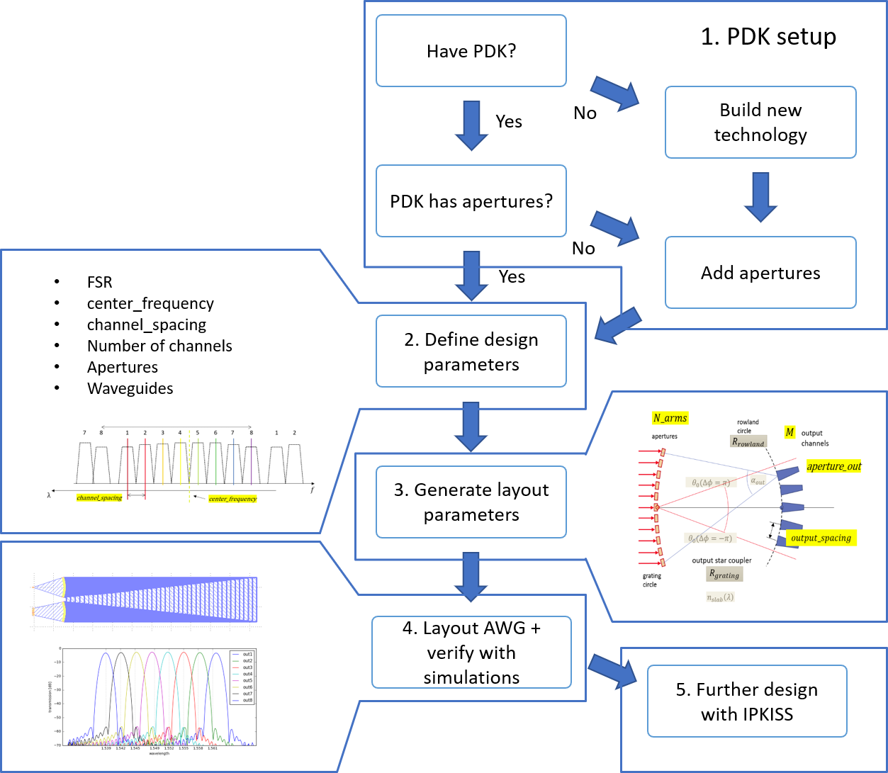
1. PDK setup
First you need to have a PDK with the proper waveguide models and apertures.
Waveguide models: in order to properly model the delay lines, a good dispersive model (preferably with phase errors) is required.
Apertures are tapers which open in a slab (free propagation region). They have additional models attached to them, which are used for the simulation of the slab region.
The table below summarizes which steps need to be taken:
Have apertures |
Don’t have apertures |
|
|---|---|---|
Have PDK |
Nothing |
Build aperture PCells.
See for example the code of |
Don’t have PDK |
Build a new PDK / technology. See also the technology guide: Technology |
Build aperture PCells + technology |
2. Reviewing the subcomponents
After the PDK is set up, subcomponents (slab template, apertures and waveguide model) need to be reviewed.
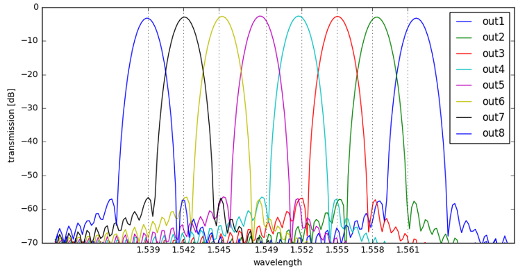
2. Synthesize the AWG device
Next step is to define your functional specifications and fab and optical rules. This means you need to choose the free spectral range, channel spacing, and several layout parameters for the apertures, grating pitch, and so on. Based on this, the AWG devices are synthesized: implementation parameters are derived, such as angles, positions, radii, delay length.
The two images below summarize the required information. In yellow are the inputs. In grey are the outputs.
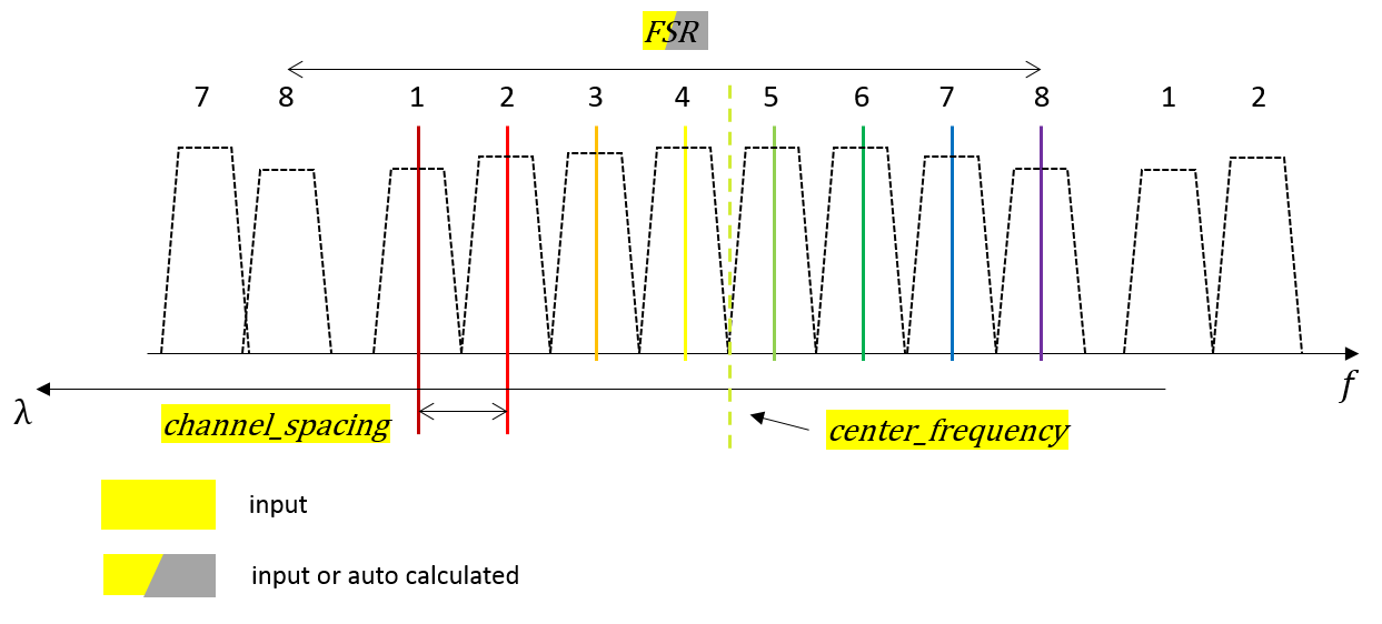
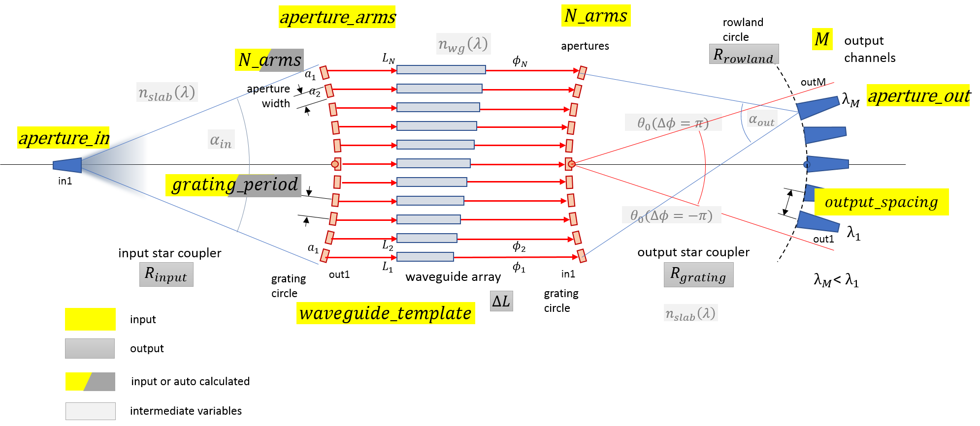
You can use the method get_layout_params_1xM_demux_um() to calculate the implementation parameters.
3. Implement the AWG
Once you have the implementation parameters, you can start creating the building blocks of the Arrayed Waveguide Grating: the star coupler and waveguide array.
4. Preparing for tape-out
As a last step, the AWG design is finalized so that it can be easily integrated with the rest of the circuit. Design errors are corrected by applying patches on sharp angles, the layout is flattened to snapping errors, and the inputs and outputs are routed to Manhattan directions.
5. Incorporating into a circuit
Once you designed your AWG, you can reuse all existing ipkiss functionality to further continue designing:
Use any IPKISS container to further route the AWG inputs / outputs. See containers.
Attaching grating couplers.
Placing in columns of grating couplers iofibcoup.
Build sweeps of AWGs with varying parameters.
Build more complex circuits with AWGs as subcells, from layout to circuit simulation with caphe. The samples contain an example of a circuit simulation, too.
Organize your AWGs in reusable libraries.
Using as part of designs in L-Edit.