Creating a new design based on a PDK
This tutorial demonstrates how to create a new design cell by placing cells from a library and routing waveguides. The tutorial is based on our si_fab demonstration PDK, but the same principle can be applied to one of our supported PDKs.
Step 1: Start a new design
Starting point: L-Edit has been launched from Luceda Control Center. No library or design is open. Start a new design by choosing from the menu or press Ctrl-n (Figure Creating a new design.).
Choose OpenAccess as the Database and enter a name and the desired path in which the new design library will be created (Figure New design using an OpenAccess database). Since we will base this design on a Process Design Kit (PDK), select OpenAccess attached library as Technology reference. The new design will then automatically use the selected technology.
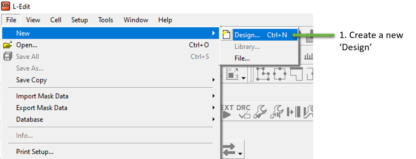
Creating a new design.
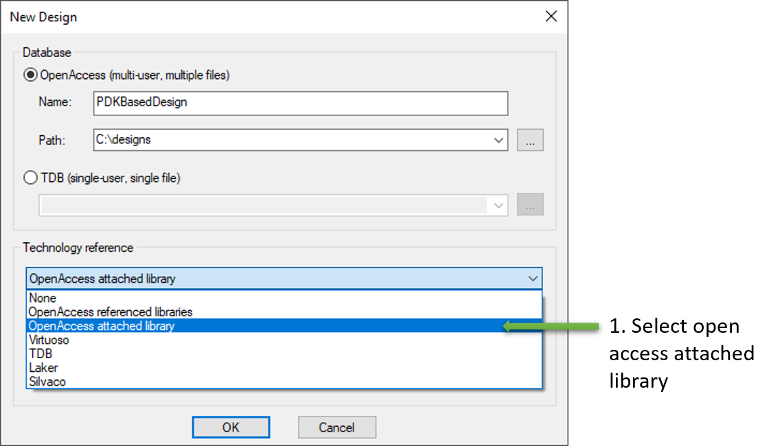
Creating a new design using an OpenAccess database with an OA attached technology library.
In the next dialog box (Figure lib.defs file) you need to specify lib.defs file location. This file contains information about all libraries that will be included in your design. Choose to create a new one in the default location:
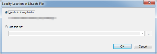
Specify the location to the lib.defs file.
Next (Figure Attach PDK library), select the technology library of choice and set it to be the Attached Library by pressing the Set button. At first, the list of Available technology libraries is empty. Add your PDK library using the Add button. In the Open dialog box, dive into the openaccess folder inside the IPKISS-based PDK you have (typically provided by the foundries), and select the library folder there.
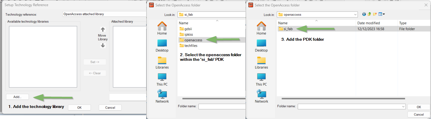
Dialog window to choose the OpenAccess attached PDK library.
After pressing OK, you should see two open libraries in the Libraries panel: the newly created design and the PDK (Figure Opened libraries), and the design layers in the Layer Palette panel (Figure Layer palette).
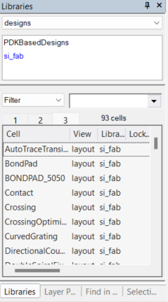
L-Edit window showing which libraries are opened.
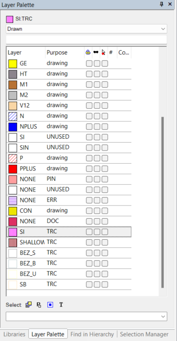
Layer palette with the layers as specified by the technology.
Step 2: Instantiate cells
Now, we will create a new cell in our (still empty) design by instantiating child cells from the PDK library. First, in the Libraries panel, make sure to select the new design (PDKBasedDesign in this example). The list of cells should still be empty. Right-click in the (empty) list of cells and select New View… from the context menu, or simply press n, to create a new cell.
In the New View dialog, enter a name for the new cell (Figure New view).
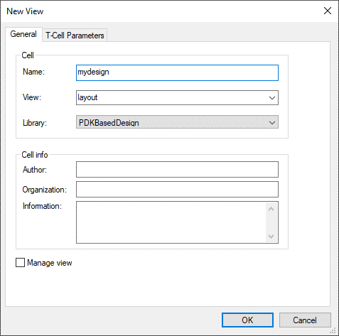
Creating a new design in the new library “PDKBasedDesign”.
Now select the PDK library from the Libraries panel and drag-and-drop the desired cells into the layout window. There are two types of cells: static cells and parametric cells (pCells). When we drag-and-drop a static cell into the new cell, a new instance of that static cell is created and their layout are immediately visualized. In case of a parametric cell, a parameter window will pop up (Figure Parameter dialog box). When user changes a parameter from its default, it turns from blue to black color.
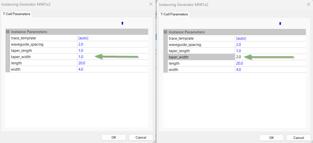
Instantiating PCells will open a new dialog box to set the parameters (note: IPKISS PCell properties are translated into L-Edit parameters).
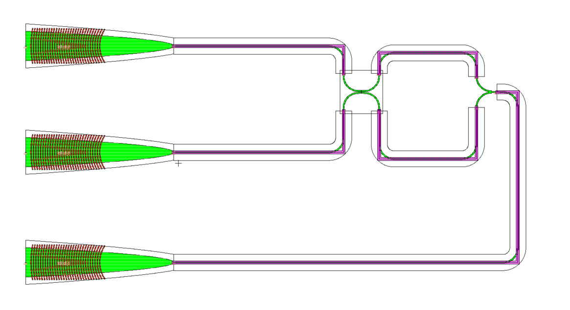
In the next example (Figure Example design), five cells were instantiated in the new design (3 fiber couplers FC_TE_1550 cells, DirectionalCoupler, and WgY90Splitter).
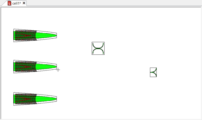
Example design after drag-and-drop of several cells from the PDK library.
Step 3: Route and generate waveguides
After the instances of library cells are placed, we can start to wire them up with waveguides. First, some setup is required:
The wire width should be set to a non-zero value in order to conveniently change the waveguide routes afterwards. Select the Wire Width drop-down from the toolbar (Figure Toolbar) and set the value, e.g. 1.0 um.
While routing waveguides, wires should snap to our cell’s pins. Select Enable Object Snap from the toolbar and then select Object Snap Pin (Figure Toolbar).

Changing the wire width so we can conveniently change the waveguide routes afterwards and enable snapping to pins.
Now, select a trace layer from Layer Palette. This is an assisting layer which has been set up in the IPKISS technology that helps routing waveguide (Figure Selecting the trace layer). For more information on how to set up these layers, please check the following section from the technology guide: Routing settings.
Each trace layer corresponds to a specific type of waveguide which will be used by default.
Then, select the All-Angle Wire tool from the toolbar (Figure All-Angle wire).
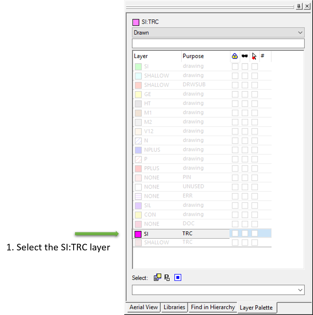
Selecting the trace layer, which is used to define waveguides.
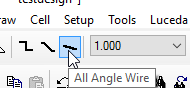
Select All-Angle Wire tool to draw waveguide control shapes on the trace layer.
We’re now ready to draw the routes of the waveguide and generate their layouts. Using the All-Angle Wire tool, we draw wires on the trace layer from one pin to another. Wires are connected to the pins easily now that Object Snap option is on.
You can now either draw a specific route, or just draw a straight line.
In case you draw a straight line, IPKISS will convert the route (if needed) into a manhattan route before generating the waveguide.
In case you draw a specific route (placing control points by mouse-clicking), IPKISS will use that route to generate the waveguide. To ensure manhattan routing when there are multiple control points hold Ctrl button and draw orthogonal sections.
In our example design, after drawing 5 routes (4 straight routes and 1 route with specified control points), the design looks like this: (Figure Connected design).
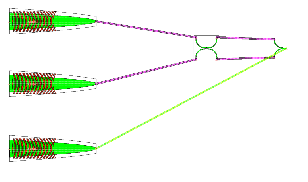
Design after cells have been connected with control shapes.
Now, select from the menu bar (Figure Generate all waveguides) or press Ctrl-Shift-w.
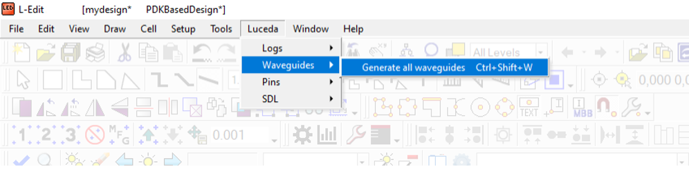
Generating all waveguides based on the drawn control shapes.
Waveguide layout is generated with the specified waveguide width and necessary roundings at bends (Figure Implemented waveguide layout).
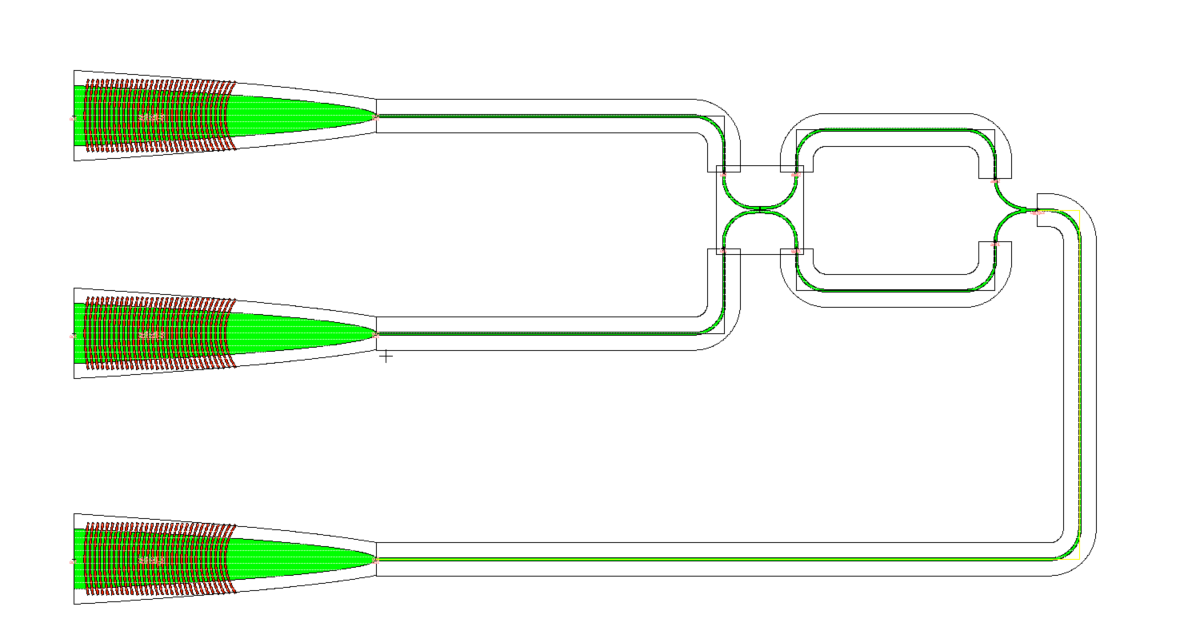
Design with the implemented waveguide layout.
Step 4: Adapt waveguide routes
If the generated waveguides are not ideal there are two ways to adapt the route and the waveguide:
Drag its trace (control shape) to the desired location (Figure Dragging an existing control shape). Select the control shape on the trace layer with mouse, drag it to the desired location and release. This method is convenient for manhattan routes (because L-Edit understands manhattan wires and assists in re-drawing properly).
Edit its control shape manually (Figure Manually updating the control shape). Select the control shape on the trace layer, and press Ctrl-e. The Edit Object(s) dialog will pop up. Adapt the coordinates manually and press OK. This method is used when accurate control of the waveguide routing is needed.
In either case, press Ctrl-Shift-w to update one waveguide or all waveguides at once.
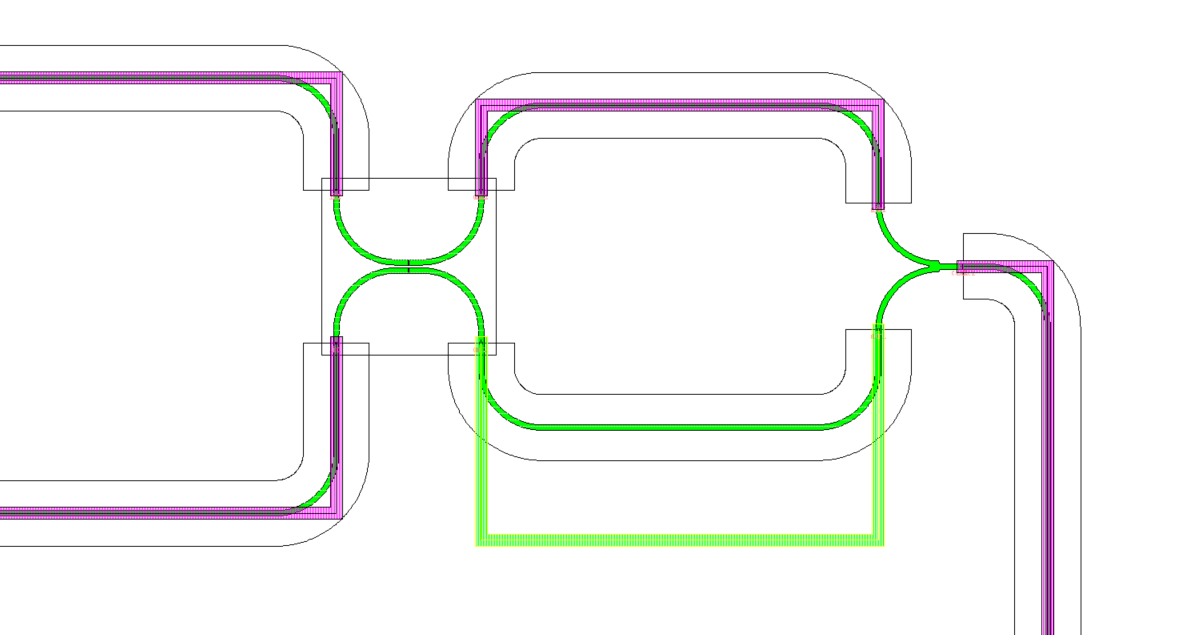
Dragging an existing control shape to update the waveguide routes.
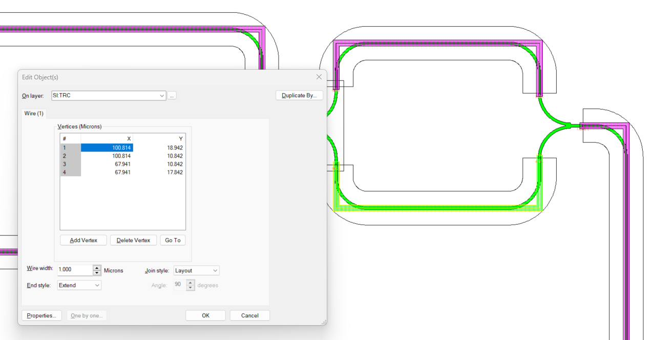
Manually updating the control shape.
After modifying the waveguide route by dragging the two traces, our example design looks like: (Figure Final design).
Design after modifying the waveguide routes.
Make sure to save the design! You can always continue the design later on: changing the location of cell instances, adapting routes and waveguides, and so forth.