LateralPNPhaseShifterTemplate
- class picazzo3.modulators.phase.trace.LateralPNPhaseShifterTemplate
PN or PIN junction phase shifter with a lateral junction. This is the most ‘classical’ type of phase shifter.
- Parameters:
- n_contact: PCell
- p_contact: PCell
- trace_template: PCell and _TraceTemplate
Refers to the other trace template from which information is taken to build this trace template.
- name: String that contains only ISO/IEC 8859-1 (extended ASCII py3) or pure ASCII (py2) characters
The unique name of the pcell
Views
- class Layout
- Parameters:
- n_bridge_pitch: float
pitch of the N-to-NPLUS bridge, longitudinal direction
- n_bridge_width: float
width of the N-to-NPLUS bridge, longitudinal direction. Set equal to the pitch size to obtain a continuous area.
- p_bridge_pitch: float
pitch of the P-to-PPLUS bridge, longitudinal direction
- p_bridge_width: float
width of the P-to-PPLUS bridge, longitudinal direction. Set equal to the pitch size to obtain a continuous area.
- junction_offset: float
offset of center of junction from the center of the waveguide
- n_metal1_width: float
width of metal1 in the lateral direction, N side
- n_metal1_offset: float
offset of metal1 in the lateral direction, N side
- p_metal1_width: float
width of metal1 in the lateral direction, P side
- p_metal1_offset: float
offset of metal1 in the lateral direction, P side
- n_contact_offsets: list<number > 0>
offsets of the contact plugs in the lateral direction, N side
- n_contact_pitch: float and number > 0
pitch of the contact plugs, longitudinal direction, N side
- p_contact_offsets: list<number > 0>
offsets of the contact plugs in the lateral direction, P side
- p_contact_pitch: float and number > 0
pitch of the contact plugs, longitudinal direction, P side
- n_silicide_extension: float
extension of the silicide area from the trace in longitudinal direction, N side
- n_silicide_width: float
width of the silicide area, in lateral direction, N side
- n_silicide_offset: float
offset of the silicide area from the centerline in lateral direction, N side
- p_silicide_extension: float
extension of the silicide area from the trace in longitudinal direction, P side
- p_silicide_width: float
width of the silicide area, in lateral direction, P side
- p_silicide_offset: float
offset of the silicide area from the centerline in lateral direction, P side
- nplus_extension: float
extension of the P++ area from the trace in longitudinal direction
- nplus_width: float
width of the N++ area, in lateral direction
- nplus_offset: float
offset of the N++ area from the centerline in lateral direction
- n_width: float and Real, number and number >= 0
width of the N+ area, in lateral direction
- pplus_extension: float
extension of the P++ area from the trace in longitudinal direction
- pplus_width: float
width of the P++ area, in lateral direction
- pplus_offset: float
offset of the P++ area from the centerline in lateral direction
- p_width: float and Real, number and number >= 0
width of the P+ area, in lateral direction
- nplus_purpose: PatternPurpose
N++ drawing purpose
- n_purpose: PatternPurpose
N+ drawing purpose
- pplus_purpose: PatternPurpose
P++ drawing purpose
- p_purpose: PatternPurpose
P+ drawing purpose
- metal1_purpose: PatternPurpose
metal1 drawing purpose
- silicide_purpose: PatternPurpose
silicide drawing purpose
- nplus_process: ProcessLayer
N++ implant process, in the contacted area
- n_process: ProcessLayer
N+ implant process (junction)
- pplus_process: ProcessLayer
P++ implant process, in the contacted area
- p_process: ProcessLayer
P+ implant process (junction)
- metal1_process: ProcessLayer
metal1 process
- silicide_process: ProcessLayer
silicide process, in th contacted area
- flipped: ( bool, bool_ or int )
flips P and N side
- junction_overlap: float
overlap of P and N regions. Set to a negative value to obtain a PIN junction
- metal_windows: List with type restriction, allowed types: <class ‘ipkiss3.pcell.trace.window.window._TraceWindow’>
List of Trace Windows for the metallization layers
- contact_windows: List with type restriction, allowed types: <class ‘ipkiss3.pcell.trace.window.window._TraceWindow’>
List of Trace Windows for the contacts
- implant_windows: List with type restriction, allowed types: <class ‘ipkiss3.pcell.trace.window.window._TraceWindow’>
List of Trace Windows for the implant layers
- windows_for_ports: List with type restriction, allowed types: <class ‘ipkiss3.pcell.trace.window.window._TraceWindow’>
List of Trace Windows from which ports will be generated
- core_width: float and number > 0
width of the waveguide core
- core_layer: __Layer__
layer used to define the core of the waveguide
- flatten_contents: ( bool, bool_ or int )
if True, it will insert the referred trace as elements in the layout, rather than as an Instance
- pin_shape: Shape
shape to be used for the pins
- trace_template_for_ports: _TraceTemplate.Layout
Trace template to be used for the ports. Default = this template
- windows: List with type restriction, allowed types: <class ‘ipkiss3.pcell.trace.window.window._TraceWindow’>
List of Trace Windows to draw on top of the already defined TraceTemplate
- keep_original_trace_template: ( bool, bool_ or int )
- width: float and Real, number and number >= 0
- control_shape_layer: __Layer__
layer on which the control shape is drawn
- draw_control_shape: ( bool, bool_ or int )
draws the control shape on top of the waveguide
- cover_layers: List with type restriction, allowed types: <class ‘ipkiss.primitives.layer.Layer’>
layers that can be used to generate additional coverage of the trace (e.g. manhattan corners)
- view_name: String that contains only alphanumeric characters from the ASCII set or contains _$. ASCII set is extended on PY3.
The name of the view
Examples
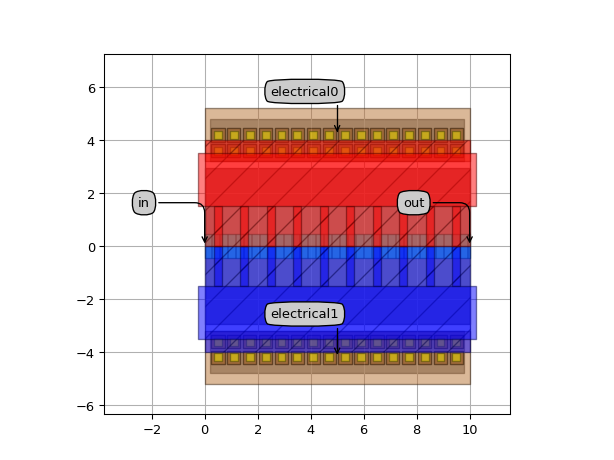
"""PN phase shifter"""
import si_fab.all as pdk  # noqa: F401
import ipkiss3.all as i3
from picazzo3.modulators.phase import LateralPNPhaseShifterTemplate
from picazzo3.traces.rib_wg import RibWaveguideTemplate
from picazzo3.electrical.contact import ContactHole

wire_t = RibWaveguideTemplate()
wire_t.Layout(core_width=0.9, cladding_width=2 * i3.TECH.WG.TRENCH_WIDTH + 0.9)

c = ContactHole(name="LPNPS_CONT")

ps_t = LateralPNPhaseShifterTemplate(trace_template=wire_t, p_contact=c, n_contact=c)

ps = ps_t(name="ExampleLateralPNPhaseShifterTemplate")
ps_lay = ps.Layout(shape=[(0.0, 0.0), (10.0, 0.0)])
ps_lay.visualize(annotate=True)
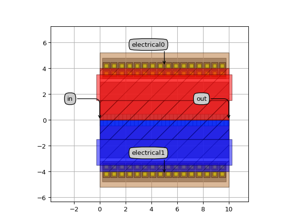
"""PN phase shifter with continuous P-PPLUS/N-NPLUS bridges"""
import si_fab.all as pdk  # noqa: F401
import ipkiss3.all as i3
from picazzo3.modulators.phase import LateralPNPhaseShifterTemplate
from picazzo3.traces.rib_wg import RibWaveguideTemplate
from picazzo3.electrical.contact import ContactHole

wire_t = RibWaveguideTemplate()
wire_t.Layout(core_width=0.9, cladding_width=2 * i3.TECH.WG.TRENCH_WIDTH + 0.9)

c = ContactHole(name="LPNPS2_CONT")

ps_t = LateralPNPhaseShifterTemplate(trace_template=wire_t, p_contact=c, n_contact=c)

ps_t.Layout(p_bridge_pitch=1.0, p_bridge_width=1.0, n_bridge_pitch=1.0, n_bridge_width=1.0)

ps = ps_t(name="ExampleLateralPNPhaseShifterTemplate2")
ps_lay = ps.Layout(shape=[(0.0, 0.0), (10.0, 0.0)])

ps_lay.visualize(annotate=True)
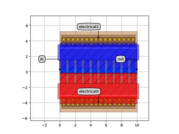
"""PN phase shifter with offset junction and overlapping P and N"""
import si_fab.all as pdk  # noqa: F401
import ipkiss3.all as i3
from picazzo3.modulators.phase import LateralPNPhaseShifterTemplate
from picazzo3.traces.rib_wg import RibWaveguideTemplate
from picazzo3.electrical.contact import ContactHole

wire_t = RibWaveguideTemplate()
wire_t.Layout(core_width=0.9, cladding_width=2 * i3.TECH.WG.TRENCH_WIDTH + 0.9)

c = ContactHole(name="LPNPS3_CONT")

ps_t = LateralPNPhaseShifterTemplate(trace_template=wire_t, p_contact=c, n_contact=c)
ps_t.Layout(
    p_bridge_pitch=1.0,
    p_bridge_width=0.6,
    n_bridge_pitch=1.0,
    n_bridge_width=0.6,
    junction_offset=0.2,
    junction_overlap=0.1,
)

ps = ps_t(name="ExampleLateralPNPhaseShifterTemplate3")
ps_lay = ps.Layout(shape=[(0.0, 0.0), (10.0, 0.0)])

ps_lay.visualize(annotate=True)

"""PN phase shifter with flipped P and N side"""
import si_fab.all as pdk  # noqa: F401
import ipkiss3.all as i3
from picazzo3.modulators.phase import LateralPNPhaseShifterTemplate
from picazzo3.traces.rib_wg import RibWaveguideTemplate
from picazzo3.electrical.contact import ContactHole

wire_t = RibWaveguideTemplate()
wire_t.Layout(core_width=0.9, cladding_width=2 * i3.TECH.WG.TRENCH_WIDTH + 0.9)

c = ContactHole(name="LPNPSF_CONT")

ps_t = LateralPNPhaseShifterTemplate(trace_template=wire_t, p_contact=c, n_contact=c)

ps_t.Layout(
    p_bridge_pitch=1.0,
    p_bridge_width=0.6,
    n_bridge_pitch=1.0,
    n_bridge_width=0.6,
    junction_offset=0.2,
    junction_overlap=0.1,
    flipped=True,
)

ps = ps_t(name="ExampleLateralPNPhaseShifterTemplateFlipped")
ps_lay = ps.Layout(shape=[(0.0, 0.0), (10.0, 0.0)])
ps_lay.visualize(annotate=True)
"""PIN phase shifter"""
import si_fab.all as pdk  # noqa: F401
import ipkiss3.all as i3
from picazzo3.modulators.phase import LateralPNPhaseShifterTemplate
from picazzo3.traces.rib_wg import RibWaveguideTemplate
from picazzo3.electrical.contact import ContactHole

wire_t = RibWaveguideTemplate()
wire_t.Layout(core_width=0.9, cladding_width=2 * i3.TECH.WG.TRENCH_WIDTH + 0.9)

c = ContactHole(name="LPINPS_CONT")

ps_t = LateralPNPhaseShifterTemplate(trace_template=wire_t, p_contact=c, n_contact=c)
ps_t.Layout(
    p_bridge_pitch=1.0, p_bridge_width=0.6, n_bridge_pitch=1.0, n_bridge_width=0.6, junction_overlap=-0.15
)

ps = ps_t(name="ExampleLateralPINPhaseShifterTemplate")
ps_lay = ps.Layout(shape=[(0.0, 0.0), (10.0, 0.0)])
ps_lay.visualize(annotate=True)
